The arcT3 · interpretationconfidence: high
Eleven grants over twenty-five years, all one discipline: using focused light to join, cut, and texture materials that conventional processes would damage. It begins with welding a ribbon and ends with atomic-scale bonds co-invented with Corning. This is the corpus's craft thread — the hands, where the feedthrough line is the cathedral those hands built.
Where it starts: the vibration problemT1 · from the patentUS6501043B1
Microelectronic connections were made by ultrasonic/thermosonic bonding — literally scrubbing parts together at high frequency. US6501043's background names the failure: vibration is "not well suited to bonding less rigid... structures," shakes parts out of position, and yields "weaker and inconsistent" bonds, while restricting usable metals. In a device where one bad joint is a surgery, that's intolerable.
The founding moveT1 · from the patentUS6501043B1
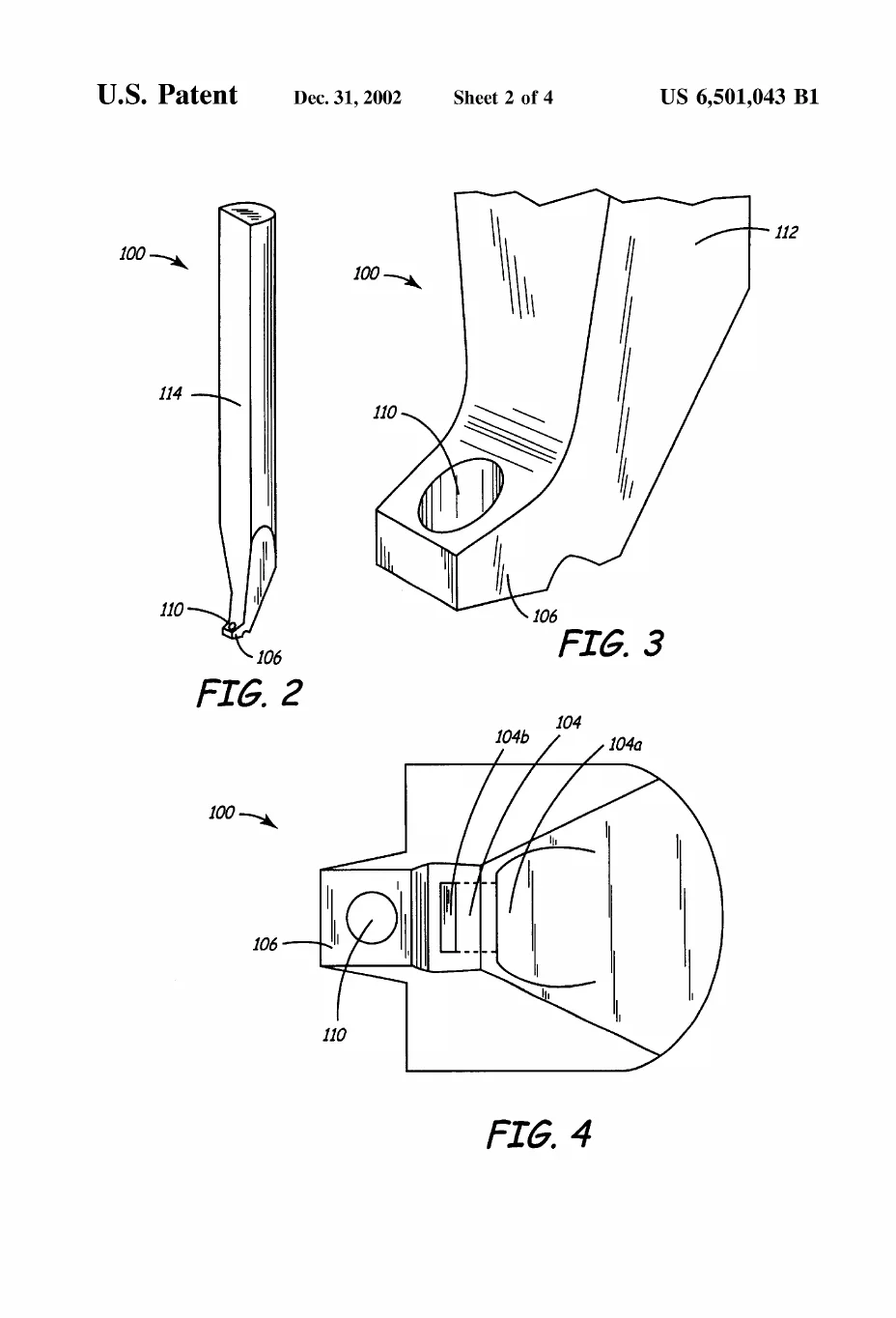
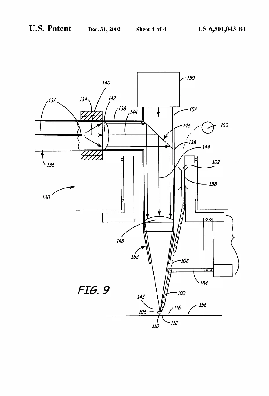
Sole inventor, claim 1: thread the ribbon under a bond head, then fire a laser through an aperture in the bond head itself, melting ribbon and pad into a single weld nugget — no vibration, no material restrictions, minimal tool wear; fiber-deliverable. The bond head holds; the light joins. Google Patents lists 35 citing patents.
Where it leadsT1 · from the patentUS10124559B2
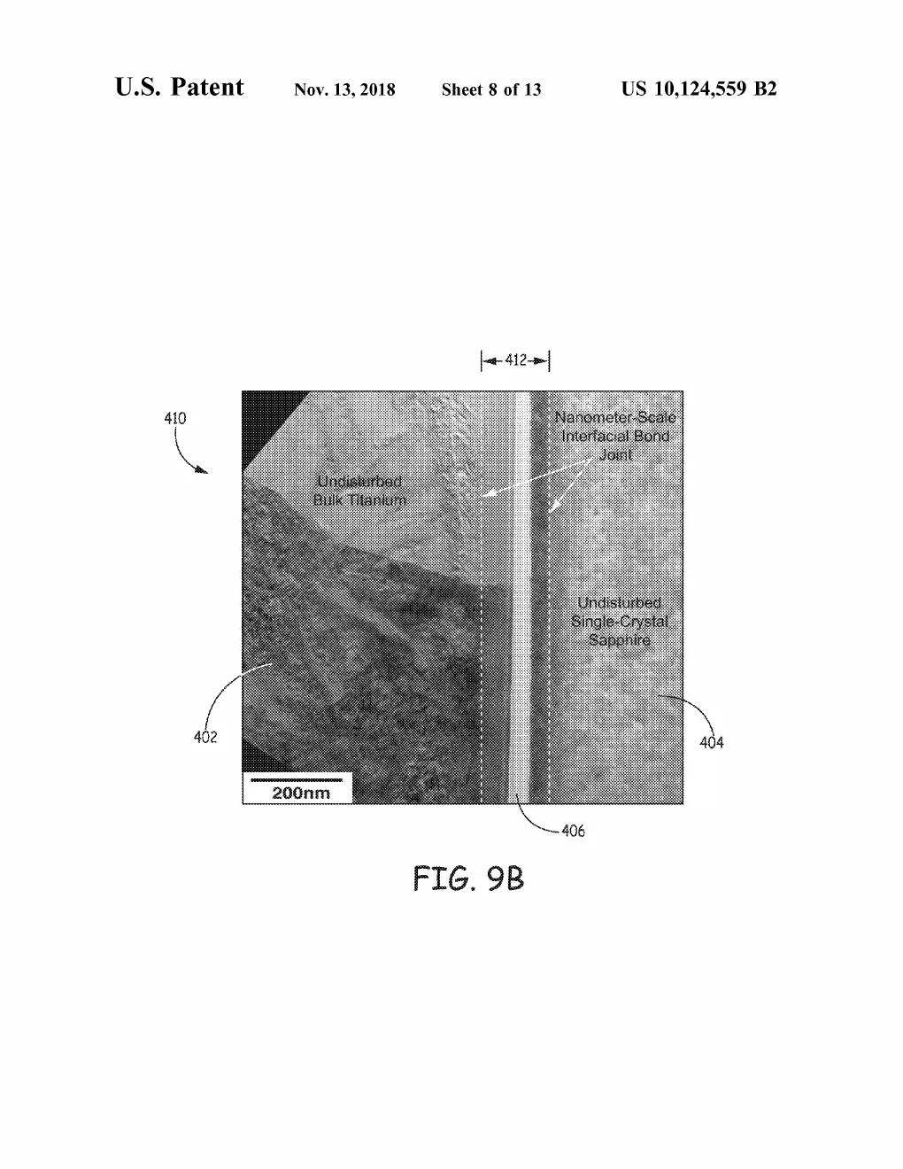
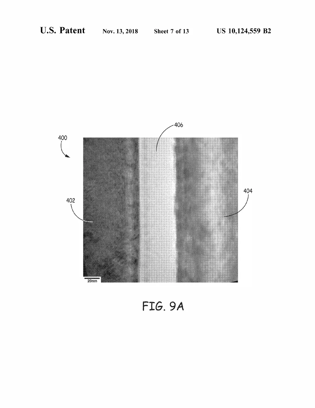
The endpoint (with Corning, US10124559 → US12454117): bond sapphire directly to titanium — transparent to opaque, insulator to metal — without the 600–1000 °C furnace such joints normally demand. The beam passes through the sapphire, deposits its energy at the interface, and forms a diffusion bond thinner than 1000 nanometers. "Kinetically limited" is the key idea: the pulse is too brief for heat to migrate, so diffusion happens only in that nano-zone — the parts never really get hot. Named applications reach past medical packaging to vacuum windows, photonics, even spacecraft. Alongside: laser-assisted direct bonding (US9171721), thin-film intermediate bonding (US8796109), two-beam laser cutting (US11999014), and underwater pulsed surface texturing (US11548092/US11969821).
Plain-English registerT3 · interpretationconfidence: high
Twenty-five years of the same magic trick at ever-smaller scale: get the heat exactly where the joint is and nowhere else. First a spot-weld through a tool's eye; finally, a bond a hundredth of a hair thick between a gem and a metal — made with a flash too fast for the heat to wander.
Cross-industry signalT2 · external source
The Corning co-assignment (US10124559, US10981355, US12454117 list both Medtronic, Inc. and Corning Incorporated as assignees — visible on the patents themselves) is the corpus's clearest external-validation marker: a materials-science giant putting its name beside his on the invention.
Set-piece note (for Presentation)T3 · interpretation
A single beam of light travels the timeline: 2000 — threading a bond head's eye to weld a ribbon; 2010 — sweeping a seam to fuse substrates; 2018 — one flash freezing into a nanometer bond between sapphire and titanium, shown at molecular zoom. The beam is the protagonist; the years are its footsteps.