The problemT1 · from the patentUS10535596B2
Every implantable device faces the same paradox: the electronics must be sealed away from body fluid absolutely, yet wires must pass through the wall to reach electrodes and sensors. That crossing point — the feedthrough — is historically the hardest joint in the device. The conventional answers, per US10535596's background: glass insulators fused to pins and ferrules by heating until the glass wets the metal, or ceramic insulators sealed by braze joints — both demanding very high temperatures, because "high temperatures are typically required to join corrosion-resistant conductive materials with corrosion-resistant insulative materials." High heat limits materials, adds bulky ferrules, and constrains how small a device can get.
The principleT1 · from the patentUS10535596B2
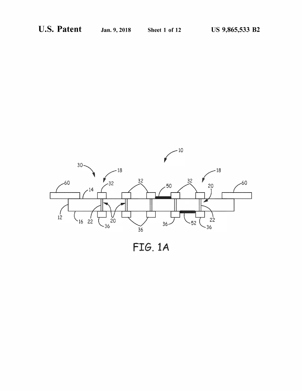
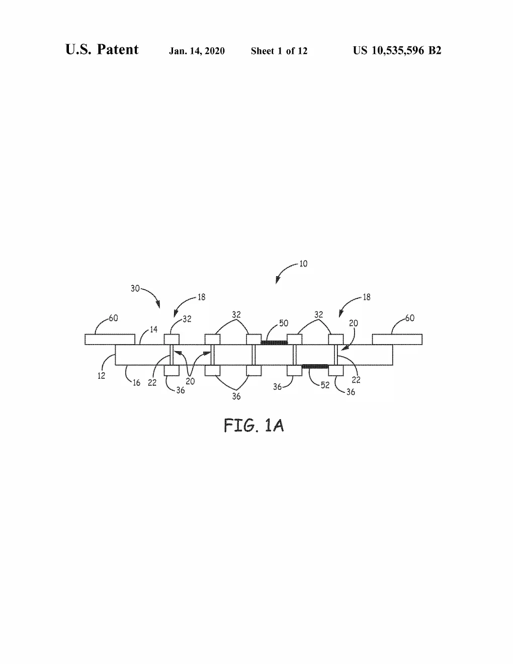
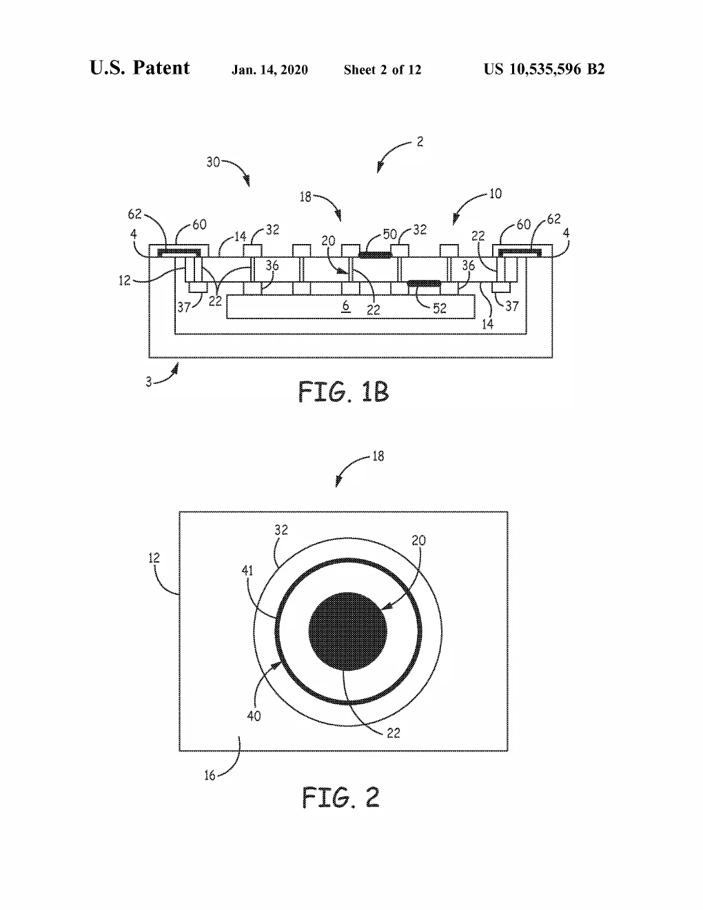
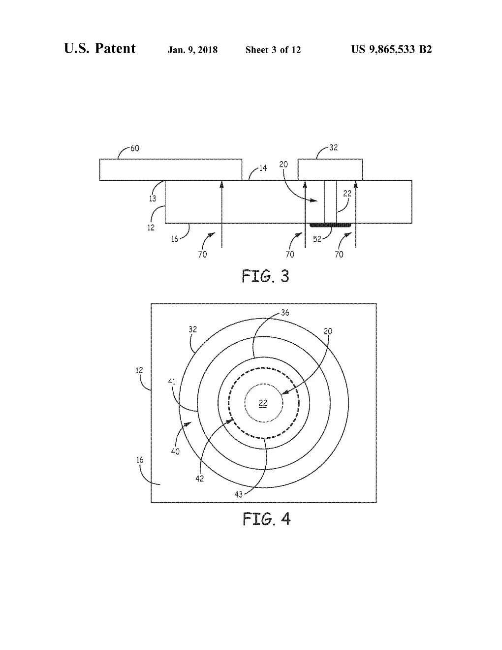
Replace furnace heat with a laser bond. The line's core claim: a non-conductive substrate with a conductive via, capped by an external contact that is hermetically sealed to the substrate by a laser bond surrounding the via — a weld whose interfacial layer can be as thin as tens of nanometers. The laser delivers energy only where the joint forms, so the bulk part stays cool: no ferrule, no braze alloy, no furnace cycle. The description's materials list shows the ambition — substrates of glass, quartz, sapphire, silicon carbide, even diamond and gallium nitride; external contacts of titanium, niobium, tantalum, platinum, iridium, stainless steel (gold appears in the via-conductor list, not the contact list).
Plain-English registerT3 · interpretationconfidence: high
Old way: bake the whole doorframe until the glass melts around the wire. His way: a spot of light traces the doorway's edge and fuses it shut — the wall never feels the heat. That's what lets the "wall" be sapphire or diamond, and the device be small.
The line itselfT1 · from the patentUS10535596B2
Twin provisional applications filed the same Christmas Eve — 62/096,677 and 62/096,699, both December 24, 2014 — seeded the line: the '677 branch became US9865533 (2018) and US10535596 (2020); the '699 branch became US10813238 (2020, sole inventor) and US11950387 (2024, sole inventor), with a further continuation published in 2024. (Corrected after adversarial QA: the branches were originally conflated into one provisional.) A decade of sustained Medtronic investment in one idea, much of it under David's name alone — and he apparently spent a Christmas Eve filing two of its foundations.
Where it sits in the corpusT3 · interpretationconfidence: high
Hermetic packaging is the largest cluster in the corpus — 20 of 56 grants — and this line is its center of gravity. It also converges his other work: the laser-bonding craft (see laser-craft) provides the joining physics; the sealed-package and pressure-sensor lines consume the feedthroughs. It is the clearest single expression of his career thesis: make the sealed box smaller, tougher, and more capable without ever compromising the seal.
Set-piece note (for Presentation)T3 · interpretation
Cross-section camera move: dive through a device wall along a single wire — outside (body fluid) → laser-traced ring bond glowing momentarily → nm-scale interface layer → inside (dry electronics). One continuous shot, six seconds, and the viewer understands what a feedthrough is forever.