The Forge · Heat IV · Hermetic Packaging & Feedthroughs · 2014-2024

The Feedthrough Line: wiring through an unbroken wall

US 9,865,533US 10,535,596US 10,813,238US 11,950,387

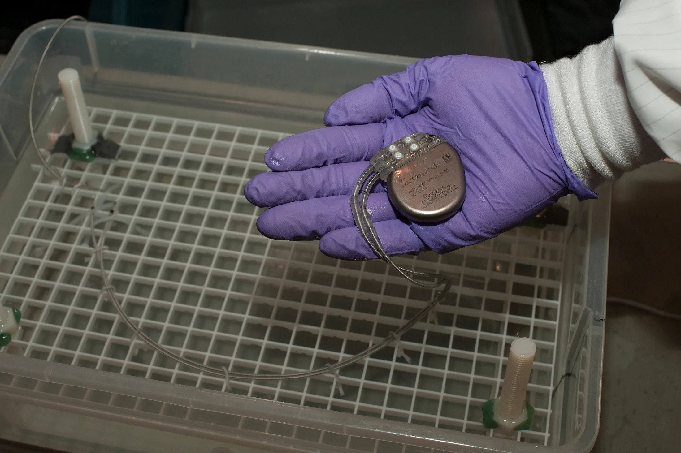
A sealed titanium pacemaker with coiled leads, held over an FDA laboratory test bath — the promise this chapter wires through an unbroken wall. — U.S. Food and Drug Administration — public domain, via Wikimedia Commons

The problemT1 · from the patentUS10535596B2

Every implantable device faces the same paradox: the electronics must be sealed away from body fluid absolutely, yet wires must pass through the wall to reach electrodes and sensors. That crossing point — the feedthrough — is historically the hardest joint in the device. The conventional answers, per US10535596's background: glass insulators fused to pins and ferrules by heating until the glass wets the metal, or ceramic insulators sealed by braze joints — both demanding very high temperatures, because "high temperatures are typically required to join corrosion-resistant conductive materials with corrosion-resistant insulative materials." High heat limits materials, adds bulky ferrules, and constrains how small a device can get.

The principleT1 · from the patentUS10535596B2

Replace furnace heat with a laser bond. The line's core claim: a non-conductive substrate with a conductive via, capped by an external contact that is hermetically sealed to the substrate by a laser bond surrounding the via — a weld whose interfacial layer can be as thin as tens of nanometers. The laser delivers energy only where the joint forms, so the bulk part stays cool: no ferrule, no braze alloy, no furnace cycle. The description's materials list shows the ambition — substrates of glass, quartz, sapphire, silicon carbide, even diamond and gallium nitride; external contacts of titanium, niobium, tantalum, platinum, iridium, stainless steel (gold appears in the via-conductor list, not the contact list).

Plain-English registerT3 · interpretationconfidence: high

Old way: bake the whole doorframe until the glass melts around the wire. His way: a spot of light traces the doorway's edge and fuses it shut — the wall never feels the heat. That's what lets the "wall" be sapphire or diamond, and the device be small.

the beam passes through the transparent part and stops at the joint Sapphire — transparent to the beam titanium < 1000 nm
Set-piece · the bond forms where the light stops

The laser-bond feedthrough, animated once as you arrive: the beam passes through the sapphire — transparent to it — and deposits its energy only at the titanium interface, where a bond line thinner than 1000 nanometers draws itself and cools from ember to dark. Static view: the finished bond, already cooled.

The line itselfT1 · from the patentUS10535596B2

Twin provisional applications filed the same Christmas Eve — 62/096,677 and 62/096,699, both December 24, 2014 — seeded the line: the '677 branch became US9865533 (2018) and US10535596 (2020); the '699 branch became US10813238 (2020, sole inventor) and US11950387 (2024, sole inventor), with a further continuation published in 2024. (Corrected after adversarial QA: the branches were originally conflated into one provisional.) A decade of sustained Medtronic investment in one idea, much of it under David's name alone — and he apparently spent a Christmas Eve filing two of its foundations.

Where it sits in the corpusT3 · interpretationconfidence: high

Hermetic packaging is the largest cluster in the corpus — 20 of 56 grants — and this line is its center of gravity. It also converges his other work: the laser-bonding craft (see laser-craft) provides the joining physics; the sealed-package and pressure-sensor lines consume the feedthroughs. It is the clearest single expression of his career thesis: make the sealed box smaller, tougher, and more capable without ever compromising the seal.
Drawing, meet reality

The claim beside the fire

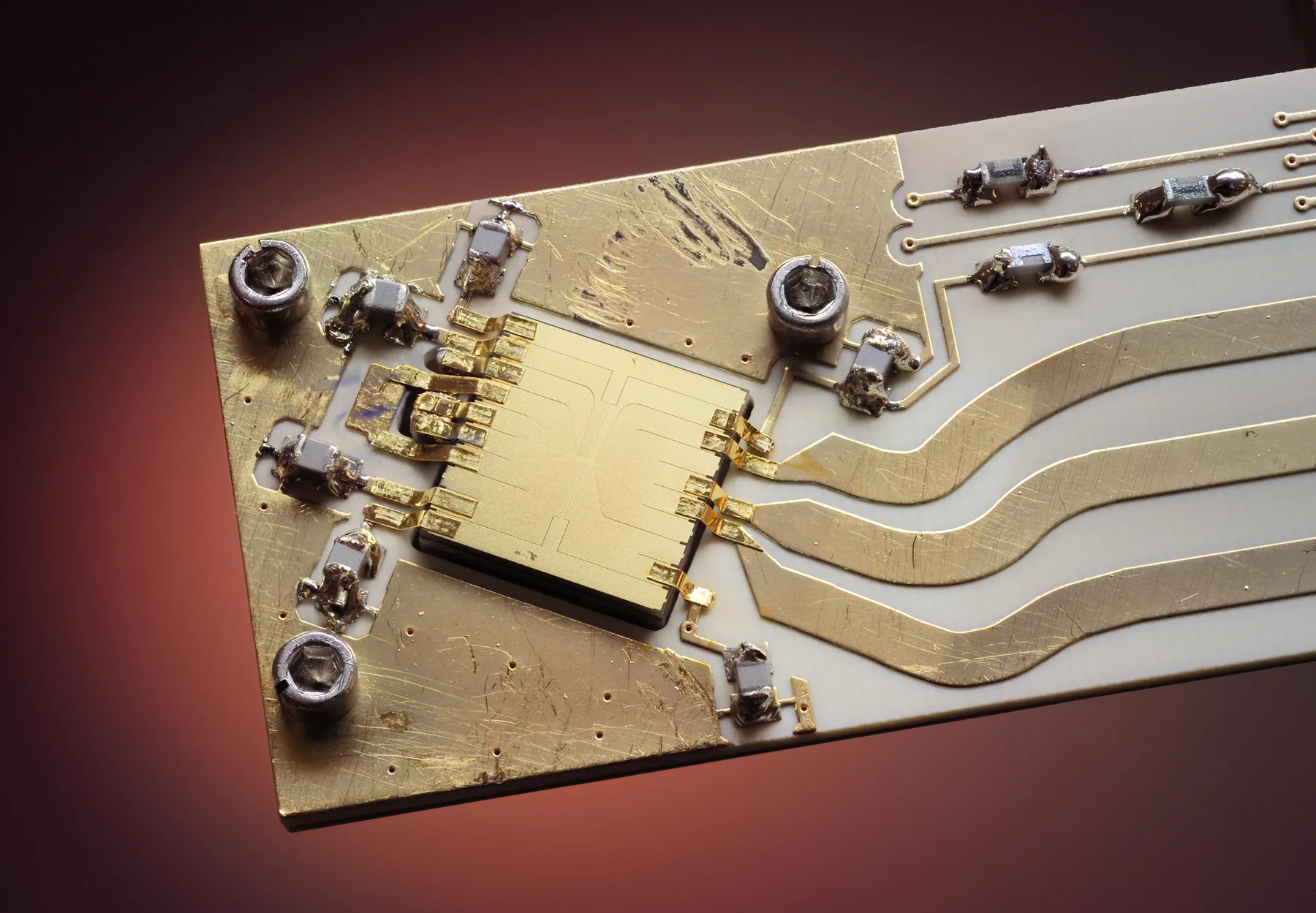
Gold ion trap on aluminum nitride backing (NIST quantum experiments)

Gold ion trap on aluminum nitride backing (NIST quantum experiments). A gold-traced chip with hand-soldered joints on aluminum nitride — conductors crossing an insulator, the feedthrough problem in miniature.

National Institute of Standards and Technology, public domain, via Wikimedia Commons
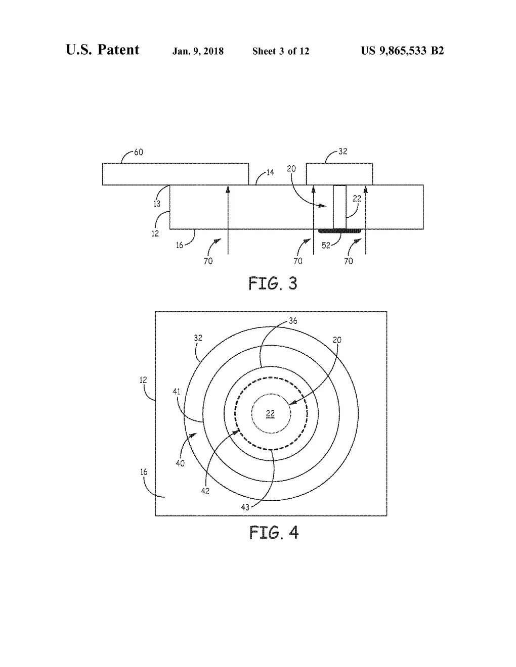
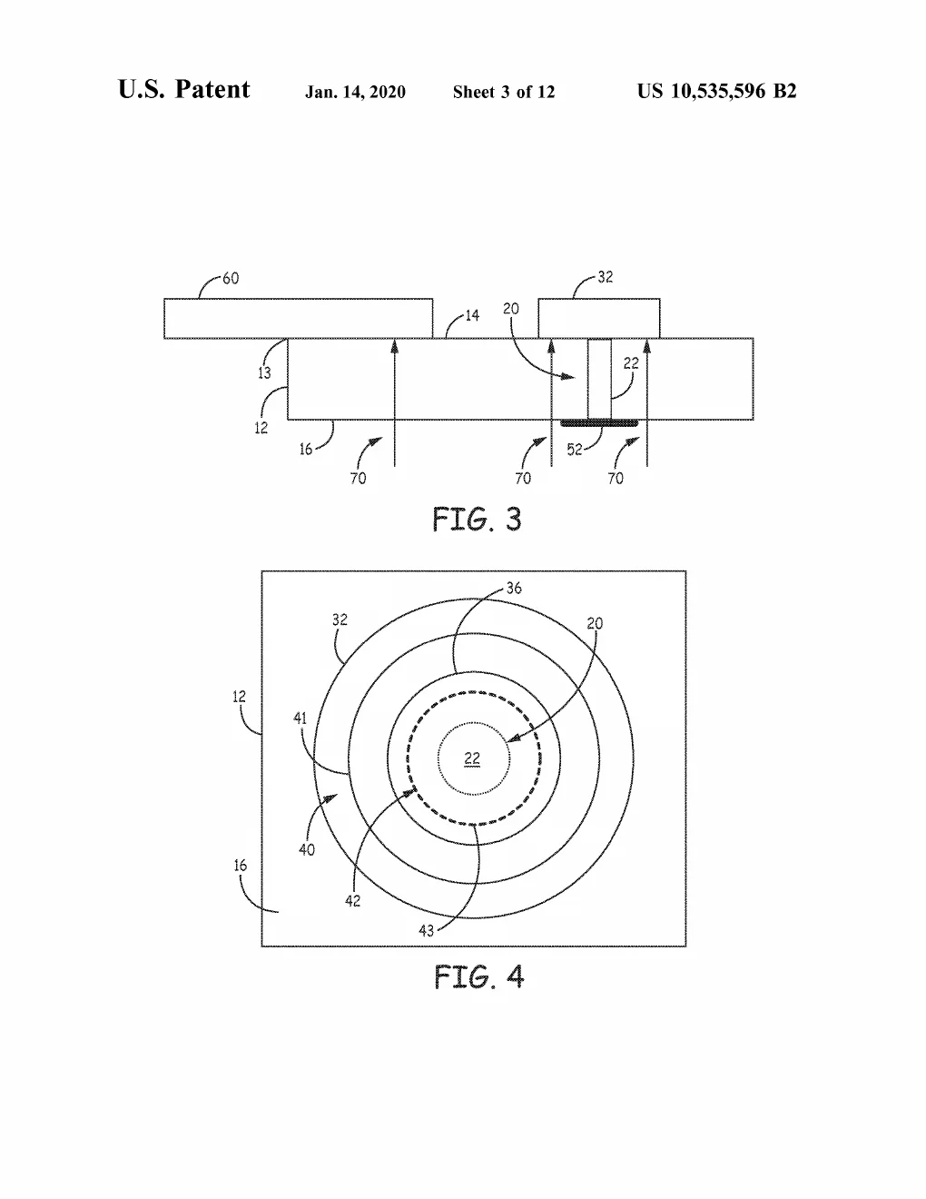
A close-up cross-section with laser-beam arrows firing up through the transparent substrate to weld a contact over its via (3), paired with a bullseye plan view of the concentric ring-shaped bond zones surrounding the wire (4).

US 10,535,596 · FIG. 3, FIG. 4 — A close-up cross-section with laser-beam arrows firing up through the transparent substrate to weld a contact over its via (3), paired with a bullseye plan view of the concentric ring-shaped bond zones surrounding the wire (4).

United States patent drawing, public domain.

Conductor through insulator, twice: the photographed gold-on-ceramic chip beside the patent sheet where laser beams fire up through a transparent substrate to seal the via they surround.

From the fire

The record in light

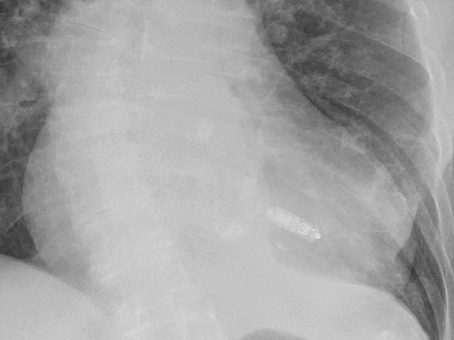
Chest X-ray with a Medtronic Micra leadless pacemaker in the heart

Chest X-ray with a Medtronic Micra leadless pacemaker in the heart. The payoff, in radiograph: a Micra leadless capsule inside a 95-year-old’s ribcage — miniaturization that only exists because signals can cross a hermetic wall.

Hellerhoff, CC BY-SA 4.0, via Wikimedia Commons
From the file

Schematics of fire

The invention in action: a cross-section with laser-energy arrows firing up through the transparent substrate to weld contact to substrate, plus a plan view of the resulting concentric ring-shaped bond lines encircling the central via like a bullseye.

US 9,865,533 · FIG. 3, FIG. 4 — The invention in action: a cross-section with laser-energy arrows firing up through the transparent substrate to weld contact to substrate, plus a plan view of the resulting concentric ring-shaped bond lines encircling the central via like a bullseye.

A text-only continuation of the patent's cover pages listing the References Cited / Other Publications, with no drawings.

US 9,865,533 · none (front matter) — A text-only continuation of the patent's cover pages listing the References Cited / Other Publications, with no drawings.

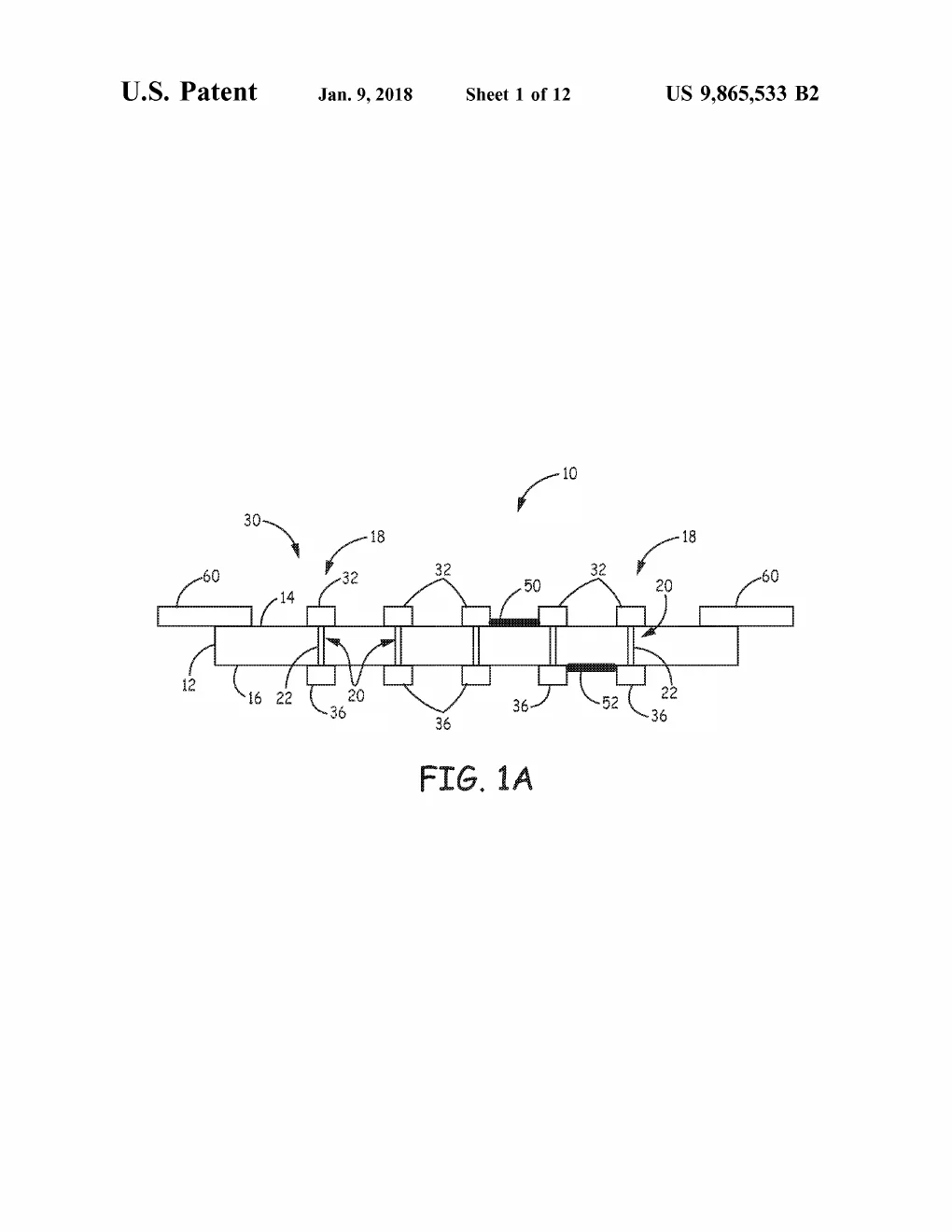
A side cross-section of the complete feedthrough assembly: a flat non-conductive substrate pierced by several conductive vias, each capped by external contacts on top and internal contacts below, with circuit elements mounted directly on the substrate surfaces.

US 9,865,533 · FIG. 1A — A side cross-section of the complete feedthrough assembly: a flat non-conductive substrate pierced by several conductive vias, each capped by external contacts on top and internal contacts below, with circuit elements mounted directly on the substrate surfaces.

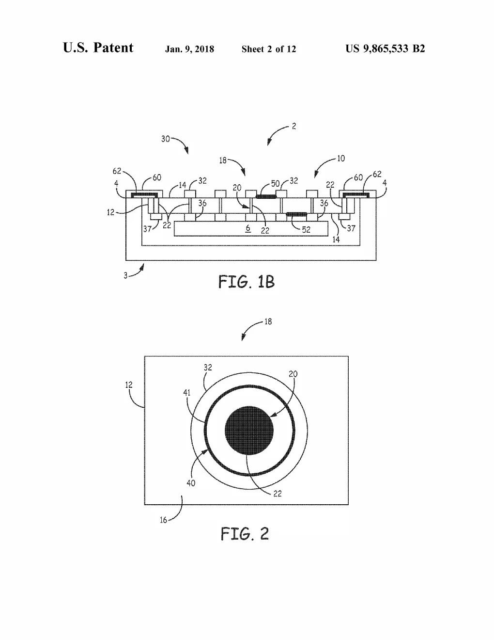
A cross-section of the feedthrough installed in an implantable device housing (electronics sealed inside, contacts facing the body) paired with a top-down view of one contact as a bullseye, the via at center ringed by the sealing bond line.

US 9,865,533 · FIG. 1B, FIG. 2 — A cross-section of the feedthrough installed in an implantable device housing (electronics sealed inside, contacts facing the body) paired with a top-down view of one contact as a bullseye, the via at center ringed by the sealing bond line.