The Pulse · Hermetic Packaging & Feedthroughs · 2014-2024

The Feedthrough Line: wiring through an unbroken wall

US 9,865,533US 10,535,596US 10,813,238US 11,950,387
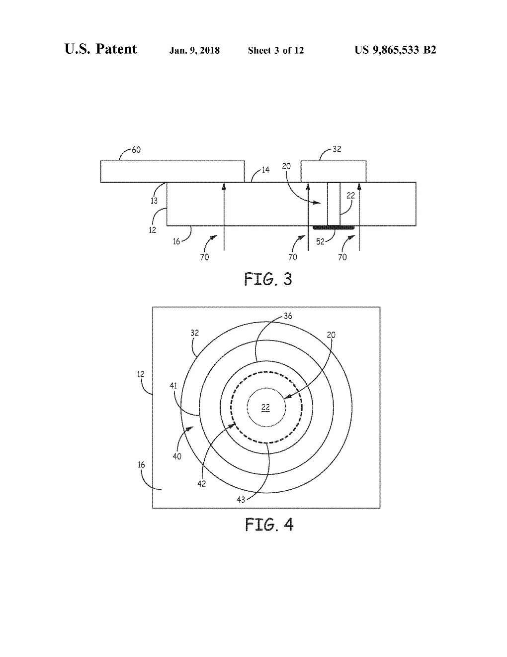
The invention in action: a cross-section with laser-energy arrows firing up through the transparent substrate to weld contact to substrate, plus a plan view of the resulting concentric ring-shaped bond lines encircling the central via like a bullseye.
From the album · US 9,865,533 · FIG. 3, FIG. 4 The invention in action: a cross-section with laser-energy arrows firing up through the transparent substrate to weld contact to substrate, plus a plan view of the resulting concentric ring-shaped bond lines encircling the central via like a bullseye.

The problemT1 · from the patentUS10535596B2

Every implantable device faces the same paradox: the electronics must be sealed away from body fluid absolutely, yet wires must pass through the wall to reach electrodes and sensors. That crossing point — the feedthrough — is historically the hardest joint in the device. The conventional answers, per US10535596's background: glass insulators fused to pins and ferrules by heating until the glass wets the metal, or ceramic insulators sealed by braze joints — both demanding very high temperatures, because "high temperatures are typically required to join corrosion-resistant conductive materials with corrosion-resistant insulative materials." High heat limits materials, adds bulky ferrules, and constrains how small a device can get.
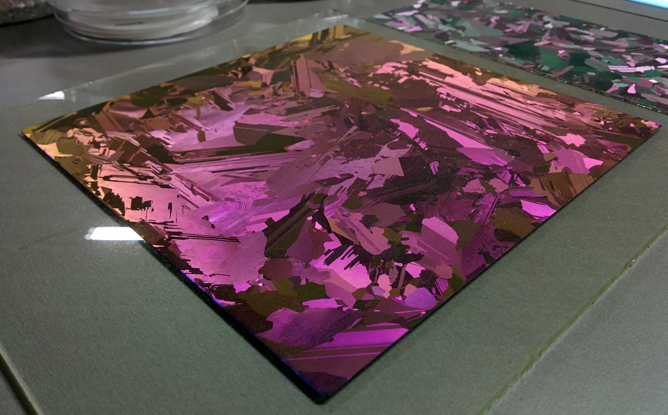
Multicrystalline silicon wafer with iridescent silicon-nitride thin film
The feedthrough problem is a thin-film problem: layers tens of nanometers deep deciding what may pass. On this silicon wafer, a nitride film one ten-thousandth of a millimeter thick is enough to repaint the whole surface — the scale at which these patents work. Multicrystalline silicon wafer with iridescent silicon-nitride thin film — Photo: Radiotrefoil, via Wikimedia Commons, CC BY-SA 4.0.

The principleT1 · from the patentUS10535596B2

Replace furnace heat with a laser bond. The line's core claim: a non-conductive substrate with a conductive via, capped by an external contact that is hermetically sealed to the substrate by a laser bond surrounding the via — a weld whose interfacial layer can be as thin as tens of nanometers. The laser delivers energy only where the joint forms, so the bulk part stays cool: no ferrule, no braze alloy, no furnace cycle. The description's materials list shows the ambition — substrates of glass, quartz, sapphire, silicon carbide, even diamond and gallium nitride; external contacts of titanium, niobium, tantalum, platinum, iridium, stainless steel (gold appears in the via-conductor list, not the contact list).

Plain-English registerT3 · interpretationconfidence: high

Old way: bake the whole doorframe until the glass melts around the wire. His way: a spot of light traces the doorway's edge and fuses it shut — the wall never feels the heat. That's what lets the "wall" be sapphire or diamond, and the device be small.

Set-piece · light tracing the seam

pulsed laser, focused at the joint titanium lid can body the seam · overlapping pulses, each spot remelting half of the last
Now bend the traveling spot into a circle. The feedthrough patents run the same pulsed laser in a closed ring around each wire’s doorway — a bullseye weld that seals the wall around the conductor without ever putting the whole assembly in a furnace.

The line itselfT1 · from the patentUS10535596B2

Twin provisional applications filed the same Christmas Eve — 62/096,677 and 62/096,699, both December 24, 2014 — seeded the line: the '677 branch became US9865533 (2018) and US10535596 (2020); the '699 branch became US10813238 (2020, sole inventor) and US11950387 (2024, sole inventor), with a further continuation published in 2024. (Corrected after adversarial QA: the branches were originally conflated into one provisional.) A decade of sustained Medtronic investment in one idea, much of it under David's name alone — and he apparently spent a Christmas Eve filing two of its foundations.
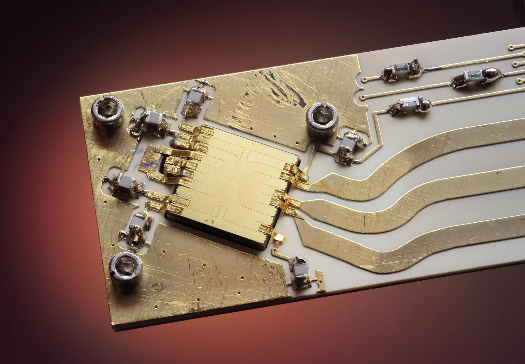
Gold ion trap on aluminum nitride backing (NIST quantum experiments)
A cousin object from another laboratory: gold conductors crossing a ceramic body, every joint deliberate. A feedthrough is exactly this discipline — precious-metal paths through an insulating wall — held to the standard of a decade in warm salt water. Gold ion trap on aluminum nitride backing (NIST quantum experiments) — National Institute of Standards and Technology, public domain, via Wikimedia Commons.

Where it sits in the corpusT3 · interpretationconfidence: high

Hermetic packaging is the largest cluster in the corpus — 20 of 56 grants — and this line is its center of gravity. It also converges his other work: the laser-bonding craft (see laser-craft) provides the joining physics; the sealed-package and pressure-sensor lines consume the feedthroughs. It is the clearest single expression of his career thesis: make the sealed box smaller, tougher, and more capable without ever compromising the seal.
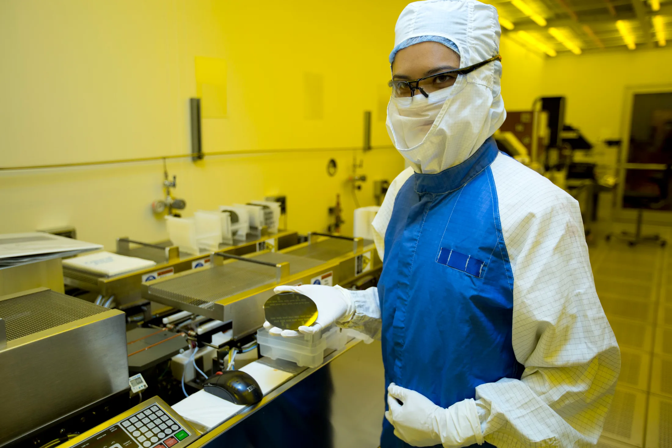
LLNL researcher in bunny suit holding a finished silicon wafer in a yellow-lit cleanroom
The hands the work passes through: a researcher in lithography-yellow light, wafer held like a communion plate. The feedthrough line ends here, in rooms where dust is the enemy and patience is the process. LLNL researcher in bunny suit holding a finished silicon wafer in a yellow-lit cleanroom — Photo: U.S. Department of Energy / Lawrence Livermore National Laboratory, public domain.

Set-piece note (for Presentation)T3 · interpretation

Cross-section camera move: dive through a device wall along a single wire — outside (body fluid) → laser-traced ring bond glowing momentarily → nm-scale interface layer → inside (dry electronics). One continuous shot, six seconds, and the viewer understands what a feedthrough is forever.

From the family album
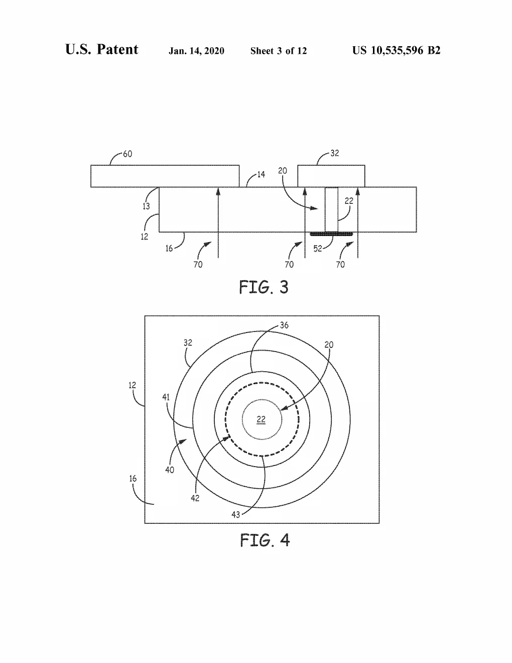
A close-up cross-section with laser-beam arrows firing up through the transparent substrate to weld a contact over its via (3), paired with a bullseye plan view of the concentric ring-shaped bond zones surrounding the wire (4).
Plate I · US 10,535,596 · FIG. 3, FIG. 4 A close-up cross-section with laser-beam arrows firing up through the transparent substrate to weld a contact over its via (3), paired with a bullseye plan view of the concentric ring-shaped bond zones surrounding the wire (4).
A text-only continuation of the patent's cover pages listing the References Cited / Other Publications, with no drawings.
Plate II · US 9,865,533 · none (front matter) A text-only continuation of the patent's cover pages listing the References Cited / Other Publications, with no drawings.
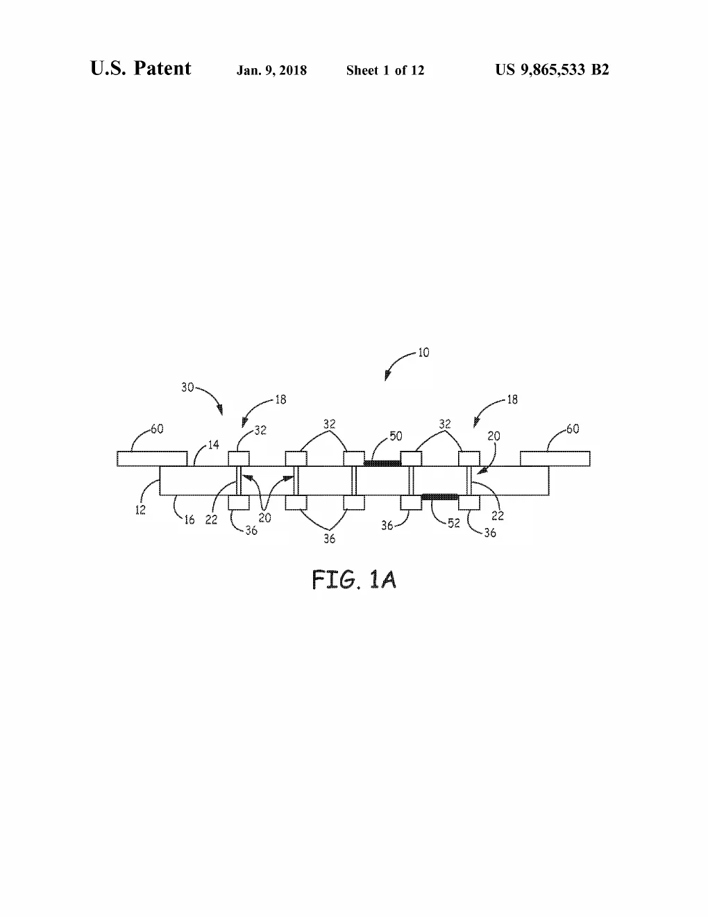
A side cross-section of the complete feedthrough assembly: a flat non-conductive substrate pierced by several conductive vias, each capped by external contacts on top and internal contacts below, with circuit elements mounted directly on the substrate surfaces.
Plate III · US 9,865,533 · FIG. 1A A side cross-section of the complete feedthrough assembly: a flat non-conductive substrate pierced by several conductive vias, each capped by external contacts on top and internal contacts below, with circuit elements mounted directly on the substrate surfaces.
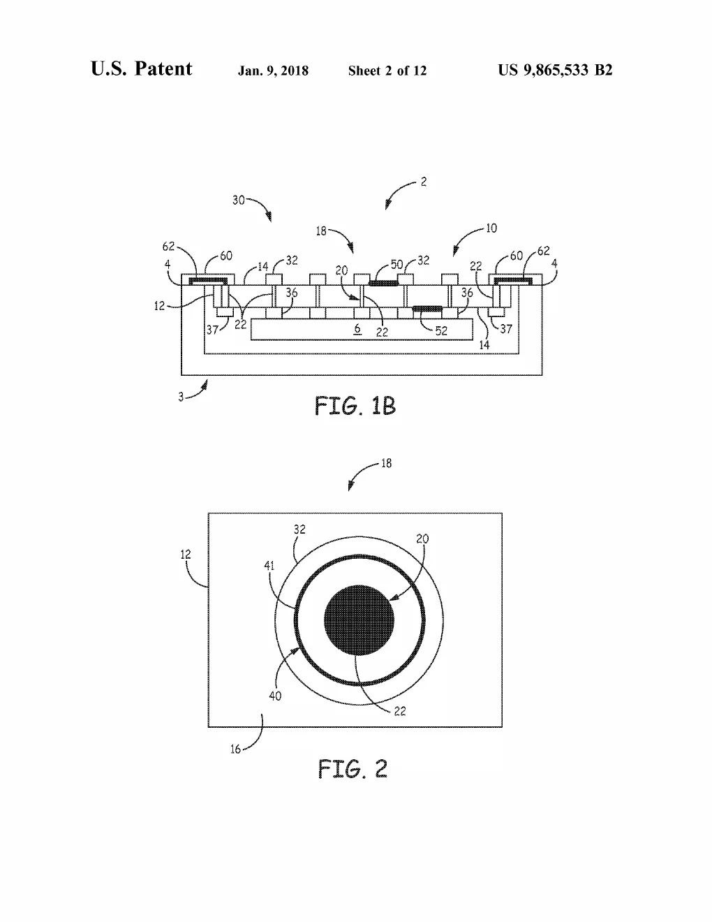
A cross-section of the feedthrough installed in an implantable device housing (electronics sealed inside, contacts facing the body) paired with a top-down view of one contact as a bullseye, the via at center ringed by the sealing bond line.
Plate IV · US 9,865,533 · FIG. 1B, FIG. 2 A cross-section of the feedthrough installed in an implantable device housing (electronics sealed inside, contacts facing the body) paired with a top-down view of one contact as a bullseye, the via at center ringed by the sealing bond line.