The Pulse · the record
Fifty-six grants, kept in time.
The complete granted corpus, in the order the world received it — from the 1993 housing filed in the era of the clam-shell can to a sealed package granted in 2026. Read it like a trace: long steady intervals, and the occasional spike.
flagship major "cited × n" = later US patents citing it as prior art · every line opens — the drawing, and the story
1990s
The origin years: the first housing, the accelerometer line, the earliest sensors. The implant is still a matchbox; the question is how to build it with fewer parts and fewer ways to fail.
4 grants
-
1996 US 5,535,097 Hermetic Packaging & Feedthroughs Implantable medical device including a first enclosure portion having a feedthrough in a second interior surface
Filed in 1993, this is where the corpus begins. Pacemakers were then built as welded clam-shells crowded with separate positioning parts; this design reshapes the can's interior so battery, circuit, and feedthrough each drop into a ready-made seat before one lid seals it shut — fewer parts, fewer steps, and a rounded contour kinder to the tissue it lives in. A hundred later patents cite it: the seed of thirty years of packaging work.
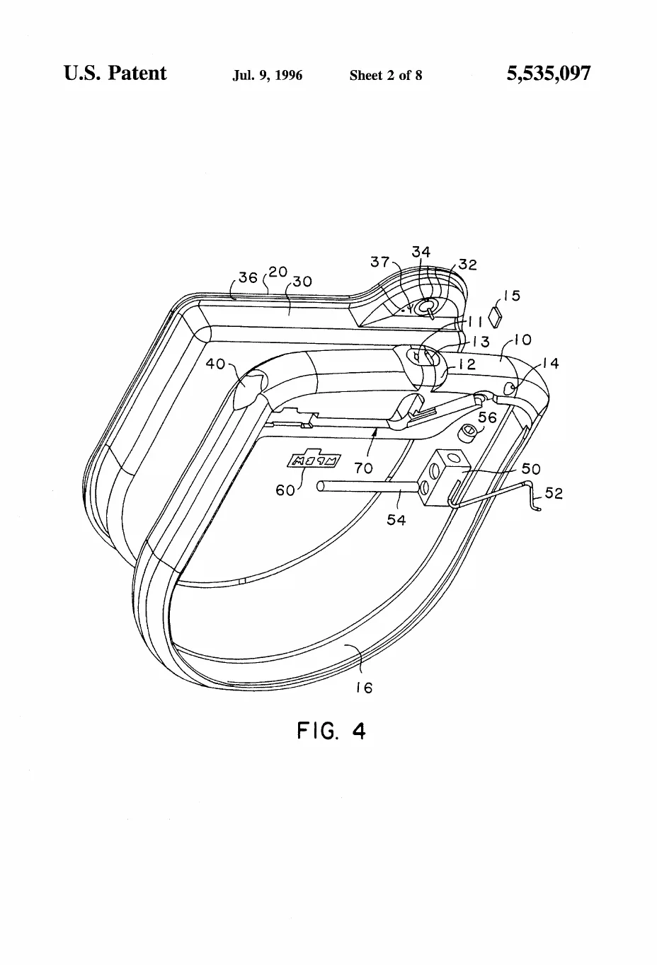
US 5,535,097 · from the drawings The lid pulled away from the shell, with connector block, setscrew, spring contact, and feedthrough floating in position — a freeze-frame of the housing assembling itself. -
1998 US 5,759,197 Hermetic Packaging & Feedthroughs Protective Feedthrough
An implanted pacemaker or defibrillator has to let electrical signals pass through its sealed metal case without ever breaking the hermetic seal that keeps body fluids out. This early Medtronic feedthrough seals a conductor pin through an insulated ferrule and adds a nearby conductive block, shaped so that an ordinary flat chip capacitor can simply bridge the two and shield the internal electronics from stray electrical and electromagnetic interference. It made electrical protection something you could bolt onto a standard sealed feedthrough instead of building a special filtered part.
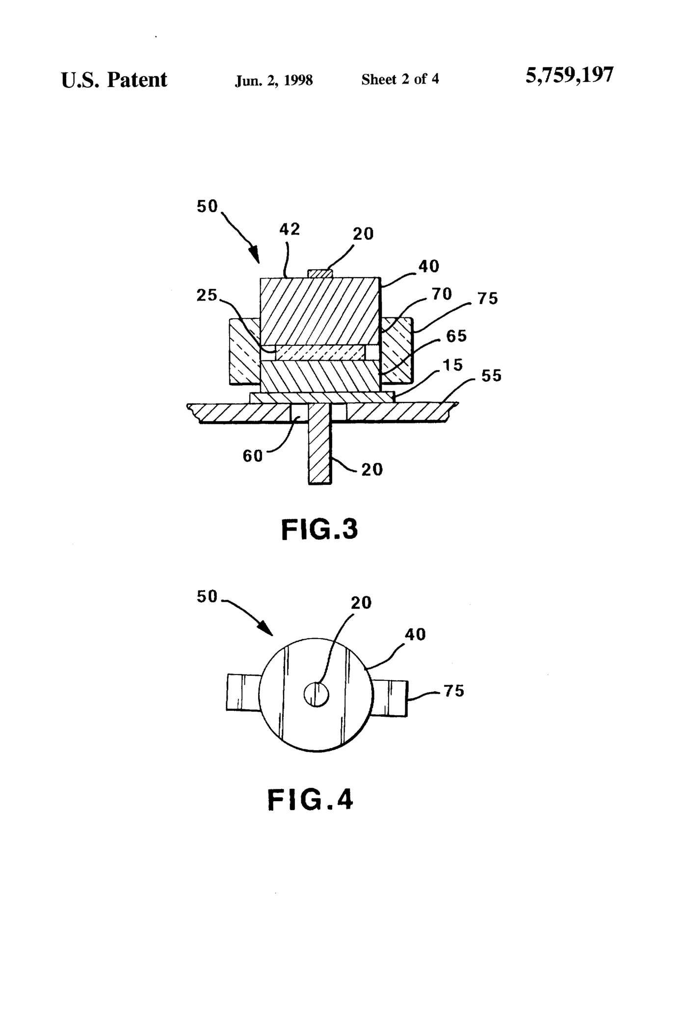
US 5,759,197 · from the drawings Cross-sectional view (FIG. 3) of the protective feedthrough: a conductor pin passes through an insulator-filled ferrule sealed in the case, while a flat chip capacitor bridges the gap between the ferrule's upstanding rim and the skirt of the conductive block above it. -
1999 US 5,885,471 Implantable Sensors Shock resistant accelerometer for implantable medical device
A rate-responsive pacemaker senses its patient's activity through a tiny piezoelectric beam — a diving board that generates voltage as it flexes — but early beams were so fragile that dropping the device from a few feet could snap them. This invention adds a stop that leaves normal flexing untouched yet catches the beam just before a shock would break it. It is the most-cited patent in the corpus, with over 200 later patents building on it.
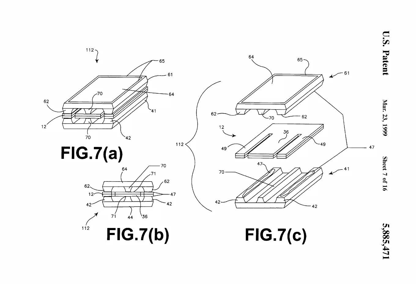
US 5,885,471 · from the drawings The shock-stop sensor in exploded stack, end-on cross-section, and assembled form — the piezoelectric beam caught between grooved plates whose center rails arrest it before a jolt can snap it. -
US 5,911,738 Implantable Sensors High output sensor and accelerometer implantable medical device
Part of the line that taught pacemakers to feel motion: a piezoelectric sensing element, built with James M. Sikorski, engineered to deliver a stronger electrical signal as it flexes with the body's movement — a clearer read on patient activity for rate-responsive pacing. With 105 citing patents, it ranks among the most-cited work in the corpus.
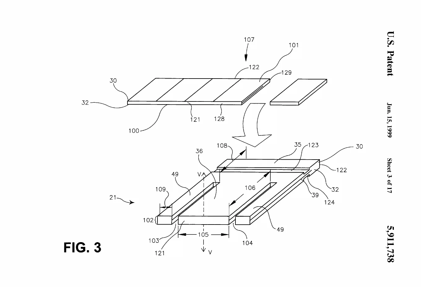
US 5,911,738 · from the drawings An exploded perspective of the sensor assembly: the piezoelectric plate, diced from a scored wafer, seated into the clamped stack that holds it.
2000s
Light becomes the joining tool, and the interconnect problem gets serious: laser bonding, terminal metallurgy, packaging that survives being made.
9 grants
-
2000 US 6,038,475 Implantable Sensors High output sensor and accelerometer for implantable medical device
The second of two grants with James M. Sikorski refining the accelerometer line's high-output sensing element — the piezoelectric beam whose flexing with body motion tells a pacemaker its patient is up and active. A continuation that sharpened the earlier design, it has been cited by 85 later patents.
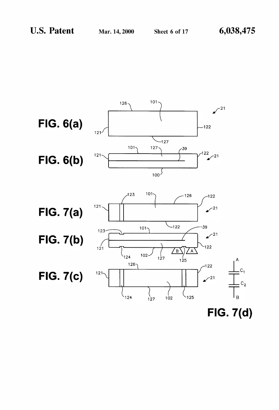
US 6,038,475 · from the drawings Side views of the sensing beam with its layered and segmented electrodes, ending in a small circuit sketch of the two capacitor sections the element forms. -
2001 US 6,216,537 Implantable Sensors Accelerometer for implantable medical device
A motion-sensing beam measures along only one axis — and the axis that matters clinically points into and out of the patient's chest, while sensors naturally lie flat on the circuit board, aiming the wrong way. This surface-mount package uses multilayer conductive end caps to stand the sensing element upright, pointing its sensitivity where medicine needs it while staying mass-producible and testable. More than 130 later patents cite the solution.
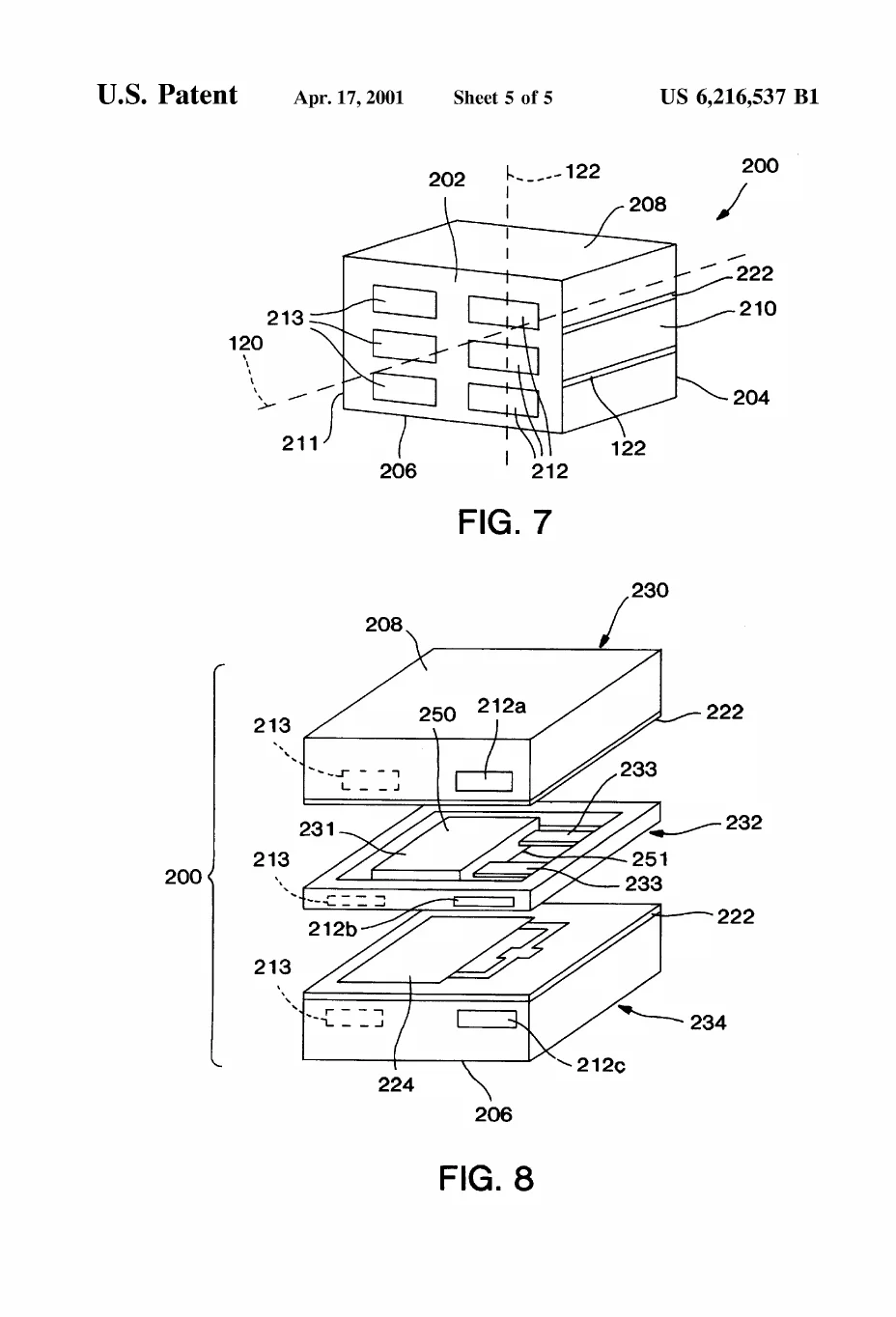
US 6,216,537 · from the drawings The assembled sensor block beside an exploded view that pops it open, revealing the tiny piezoelectric beam suspended over its cavity between two covers. -
2002 US 6,501,043 Laser Materials Processing Apparatus and method for laser welding of ribbons
Microelectronic connections were made by ultrasonic scrubbing — vibration that shook parts out of position and left weak, inconsistent bonds. Working alone, he threaded the ribbon under a bond head and fired a laser through an aperture in the tool itself: the head holds, the light joins. Thirty-five later patents cite it, and it opened a twenty-five-year arc of using focused light as a precision tool.
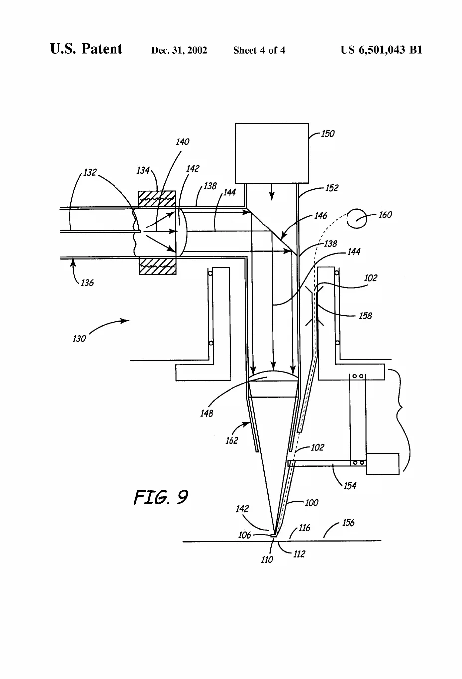
US 6,501,043 · from the drawings A cross-section of the welding apparatus, tracing the laser beam from its source, off a mirror, through a lens, and out the bond head's own aperture onto the ribbon joint. -
2004 US 6,717,100 Laser Materials Processing Apparatus and method for laser welding of ribbons
A sole-inventor continuation of the ribbon-welding patent that opened the laser-craft arc: a bond head holds a conductive ribbon in place while the laser fires through an aperture in the tool itself, so the weld forms without the vibration that used to shake delicate parts loose. The refinement went on to be cited by 38 later patents — more than the original.
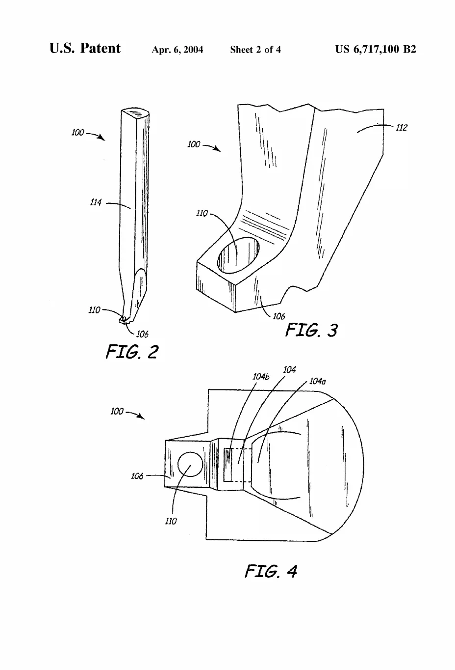
US 6,717,100 · from the drawings Perspective and magnified views of the bonding tool, revealing the aperture bored straight through its foot — the eye the laser fires through. -
US 6,787,891 Interconnects & Materials Freeform substrates and devices
Substrates come out rectangular because saws cut straight — but implantable devices are curved, so corners of precious interior volume sit empty. Ruben's sole-inventor answer, filed in 2000, was to cut the silicon freeform to the device's interior contour using a water-jet-guided laser, shaping the circuitry to match. Every reclaimed cubic millimeter is that much less bulge in a patient's chest.
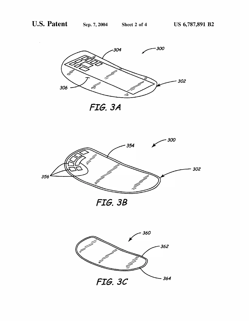
US 6,787,891 · from the drawings Three perspective views of a substrate cut and curved to hug a device's rounded interior, its chip pads riding the bend. -
2005 US 6,963,780 Interconnects & Materials Implantable medical device including a surface-mount terminal array
Welding and wire-bonding straight onto a circuit board kept damaging the board itself: solder contamination, heat cracking, costly rework. This molded terminal array is a translation layer — each terminal offers a small solder face downward for tight-pitch fillets and a large bond head upward for the bonding tools, so each joining technology gets the surface it wants. Rivals noticed: the patent has been cited roughly 31 times by effectively the whole competing pacemaker-and-neurostimulator industry, from Boston Scientific and BIOTRONIK to Verily and TDK.
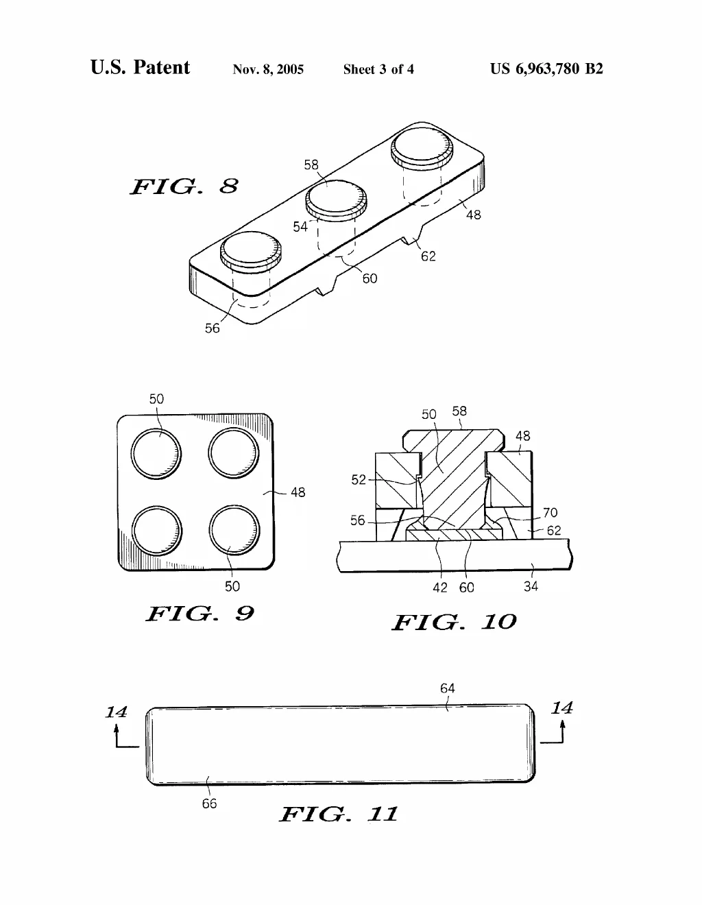
US 6,963,780 · from the drawings A 3D view of the molded terminal block with its buried terminals, beside a cross-section of one terminal — narrow solder face below, wide wire-bond head above. -
2007 US 7,288,847 Hermetic Packaging & Feedthroughs Assembly including a circuit and an encapsulation frame, and method of making the same
Encapsulant faces a paradox: it must flow freely enough to infiltrate a circuit's every crevice, yet not flood the board — and molded walls leak at post holes and cost too much. Ruben's first-listed answer is geometry: a flat frame, thermally matched to the substrate, whose through-hole corrals the encapsulant around the components, with extra openings that deliberately keep contacts and ID codes exposed for later assembly steps. A dam instead of a mold — cited 13 times, including by Shindengen.
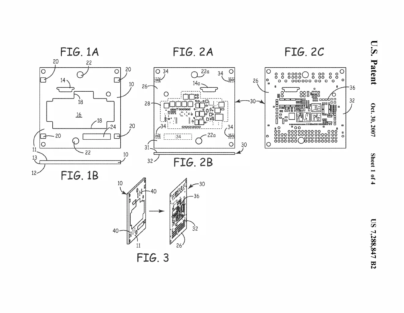
US 7,288,847 · from the drawings The frame with its window-shaped well, the circuit board it guards, and a perspective of the two being brought together. -
2008 US 7,335,530 Interconnects & Materials Freeform substrates and devices
A continuation of Ruben's sole-inventor freeform-substrates idea: instead of a rectangular circuit board leaving the corners of a curved implantable device empty, the substrate is cut to the shape of the device's interior. Even the integrated-circuit components are formed to follow that contour, freeing room for more electronics — or letting the whole device shrink.
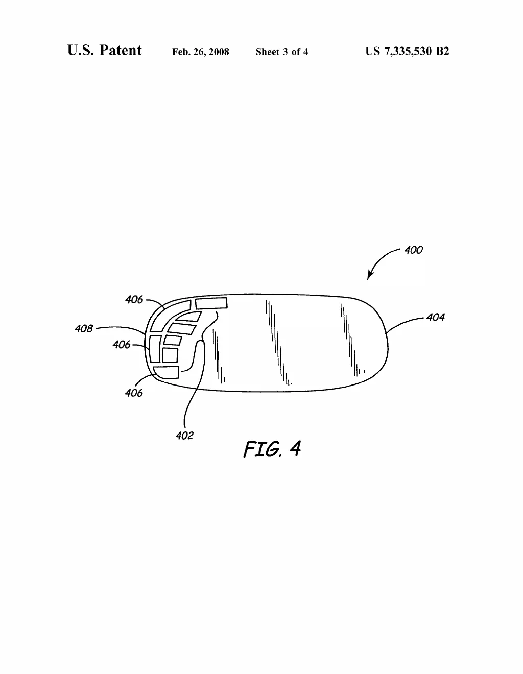
US 7,335,530 · from the drawings A view into a pill-shaped device where the circuit components fan around the rounded end instead of stopping at a rectangle's corner. -
2009 US 7,591,185 Implantable Sensors Pressure sensor configurations for implantable medical electrical leads
A cardiac lead is normally just wiring; this patent puts a working pressure sensor inside the lead itself. Behind an insulating sidewall, a pressure-sensitive diaphragm moves one plate of a tiny gap capacitor read by an on-board chip, with a grounded conductive layer shielding the measurement. It is the moment the wire becomes an instrument.
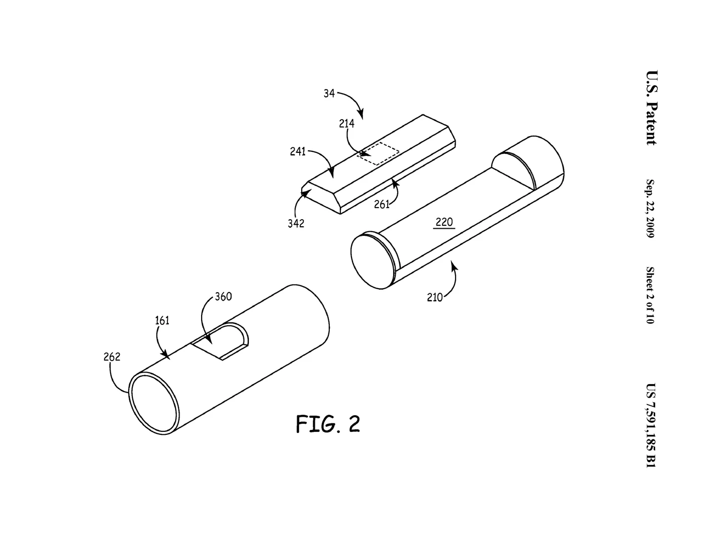
US 7,591,185 · from the drawings An exploded view of the sensor module: the block-shaped pressure sensor with its diaphragm window floating between its cradle and the lead's outer tube with a matching cutout.
2010s
Miniaturization arrives in earnest — wafer-scale packages, laser-bonded feedthroughs, sapphire windows, and the first bets on decay as a battery.
24 grants
-
2010 US 7,682,878 Hermetic Packaging & Feedthroughs Encapsulation circuitry on a substrate
Protecting a finished circuit means covering it in encapsulant that must be runny enough to seep around every component yet thick enough not to pour off the board. This continuation extends the encapsulation-frame idea: a flat frame, matched to the board's thermal expansion, whose through-hole wall dams the liquid right where it is needed. Even its extra holes are practical, leaving contacts and ID codes exposed for the next step on the production line.
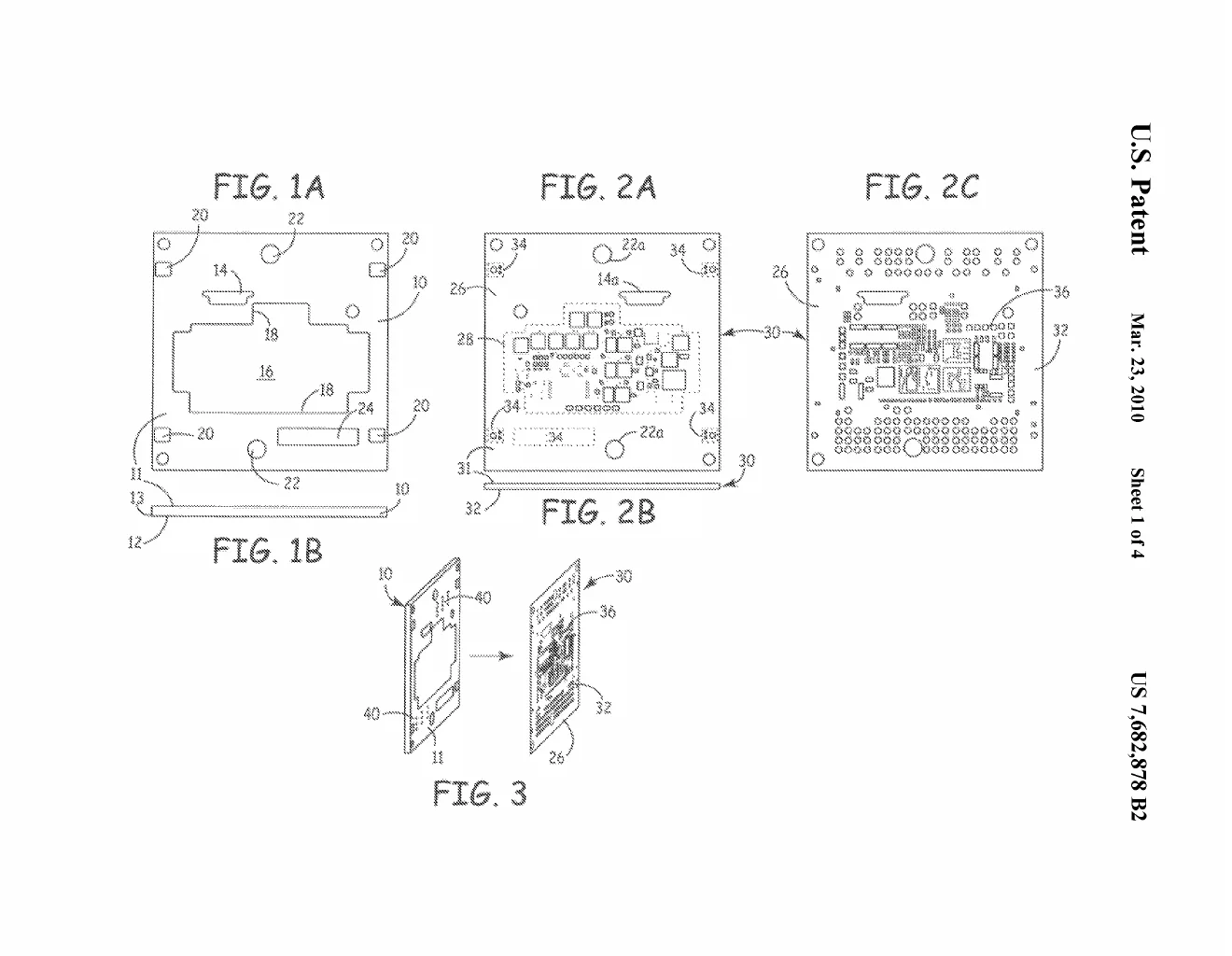
US 7,682,878 · from the drawings The flat encapsulation frame and the circuit board it protects, with a perspective view of the frame being lowered onto the populated board. -
2011 US 7,872,208 Laser Materials Processing Laser bonding tool with improved bonding accuracy
Laser bonding is only as good as the tool's aim — the weld has to land exactly where the foot is pressing. This patent, with Ruben listed first, refines the bonding tool's tip so the laser strikes its target more accurately, a workhorse improvement in his laser materials-processing line. A dozen later patents cite it.
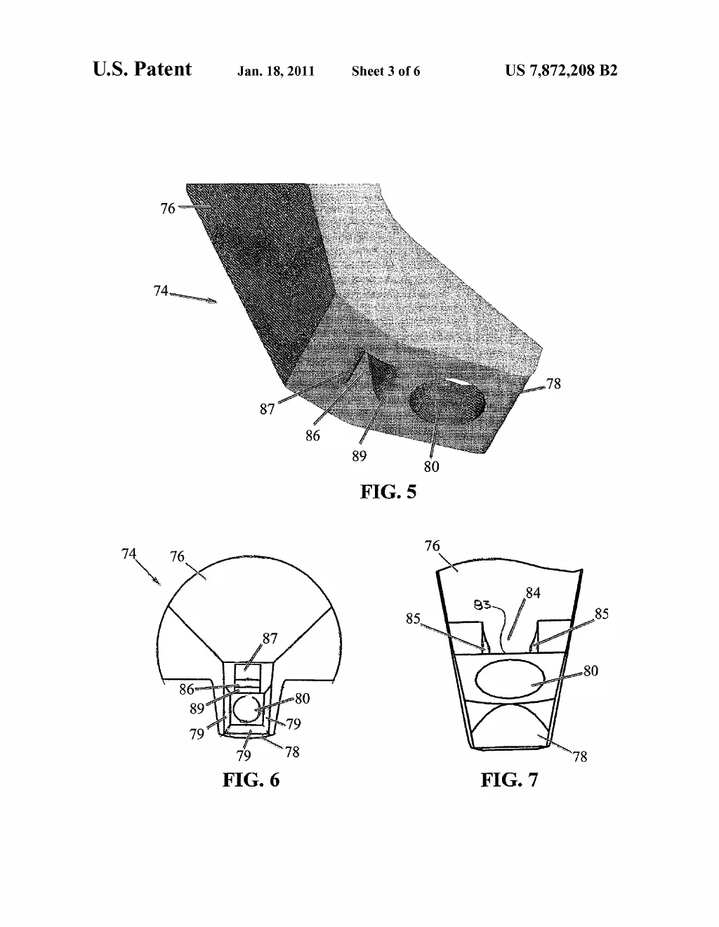
US 7,872,208 · from the drawings A shaded 3D close-up of the laser bonding tool's tip, with two end-on views revealing the opening in its foot. -
US 7,886,608 Implantable Sensors Pressure sensor configurations for implantable medical electrical leads
A cardiac lead is normally just a wire; this work builds a pressure sensor directly into it, so the wire itself becomes an instrument. Inside the lead's insulating wall, a pressure-sensitive diaphragm forms one plate of a gap capacitor read by an integrated circuit, with a grounded conductive layer shielding the diaphragm from interference. It's a continuation in a sensing line whose ideas were picked up by 46 later patent families.
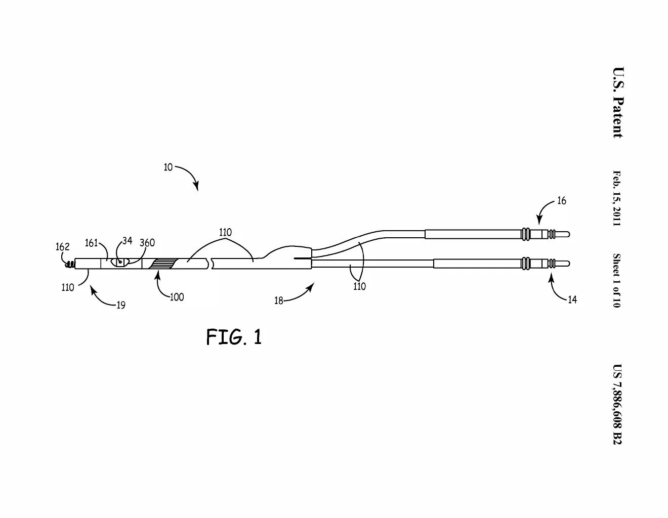
US 7,886,608 · from the drawings The full implantable lead, from its connector pins down to the inline pressure-sensor capsule near the tip. -
US 7,902,851 Hermetic Packaging & Feedthroughs Hermeticity testing
Moisture is the quiet killer of implanted electronics, and the seam between two bonded chips is exactly where a micro-package is most vulnerable — yet conventional tests can't see into that buried interface. So the test is built into the seal itself: tiny chain circuits on both chips mate at bonding into rings around each sealed region, and moisture creeping in breaks or shorts a chain at the perimeter before the electronics are ever at risk. Not making the seal — proving it, electrically, from the inside.
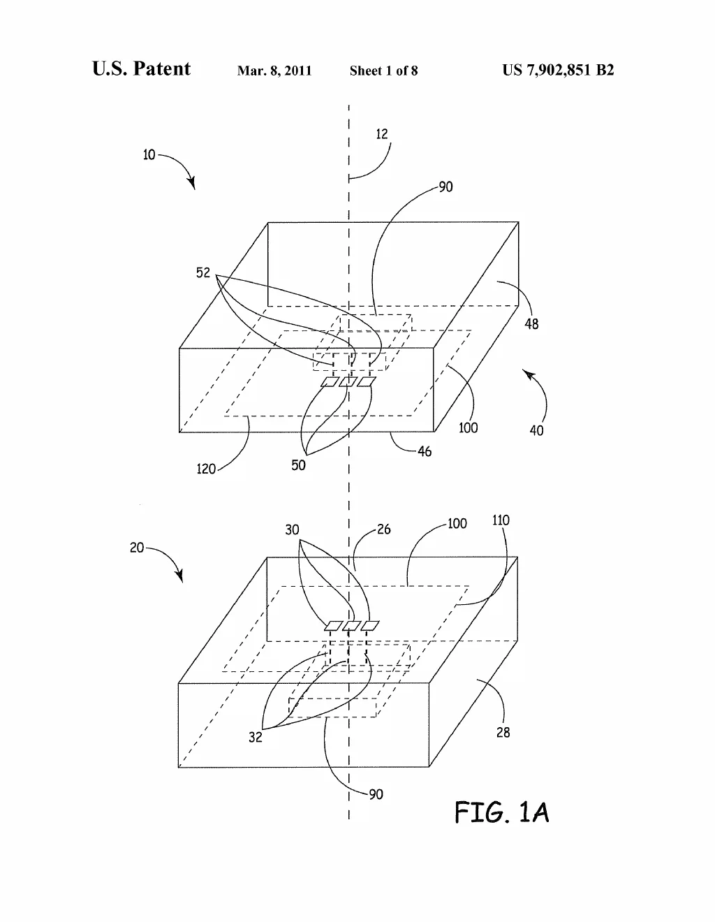
US 7,902,851 · from the drawings Two chips poised face-to-face before bonding, with the small test contacts that will mate into a seal-checking circuit around the protected region. -
2012 US 8,141,556 Interconnects & Materials Metallization with tailorable coefficient of thermal expansion
Welding a wire to a thick metal pad on silicon can crack the chip, because the heat makes pad and substrate expand at different rates. The sole-inventor answer is a composite pad containing a material that shrinks when heated — niobium and niobium pentoxide, blended so the mismatch cancels to zero — and the patent hands over the design equation as a recipe. The idea traveled: four of its visible citations come from Lockheed Martin, defense-aerospace uptake of an implant metallurgy trick.
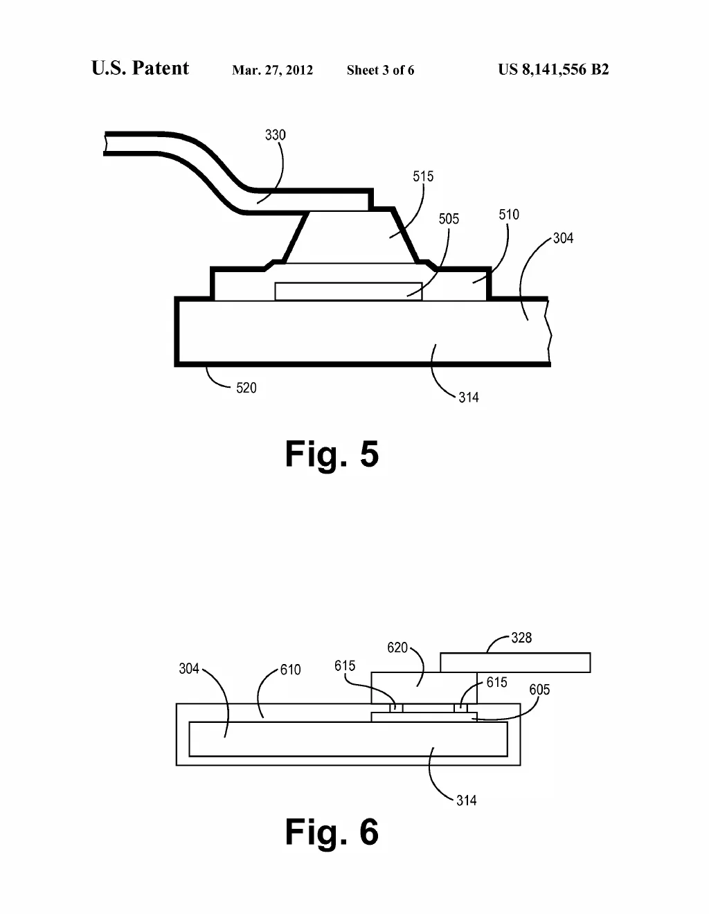
US 8,141,556 · from the drawings A cross-section of a connector ribbon welded onto the layered pad whose composite metal is tuned to expand in step with the substrate below. -
2013 US 8,424,388 Implantable Sensors Implantable capacitive pressure sensor apparatus and methods regarding same
Tiny capacitive pressure sensors are haunted by stray capacitance, and the problem is worst exactly where implants live — surrounded by conductive tissue and fluid. This design flips the obvious layout: the electrode facing the body is the grounded, pressure-flexing diaphragm, while the signal electrode sits isolated on an insulator behind it, so the patient's own conductivity becomes shielding instead of interference. Design judo — the hostile environment is recruited into the circuit.
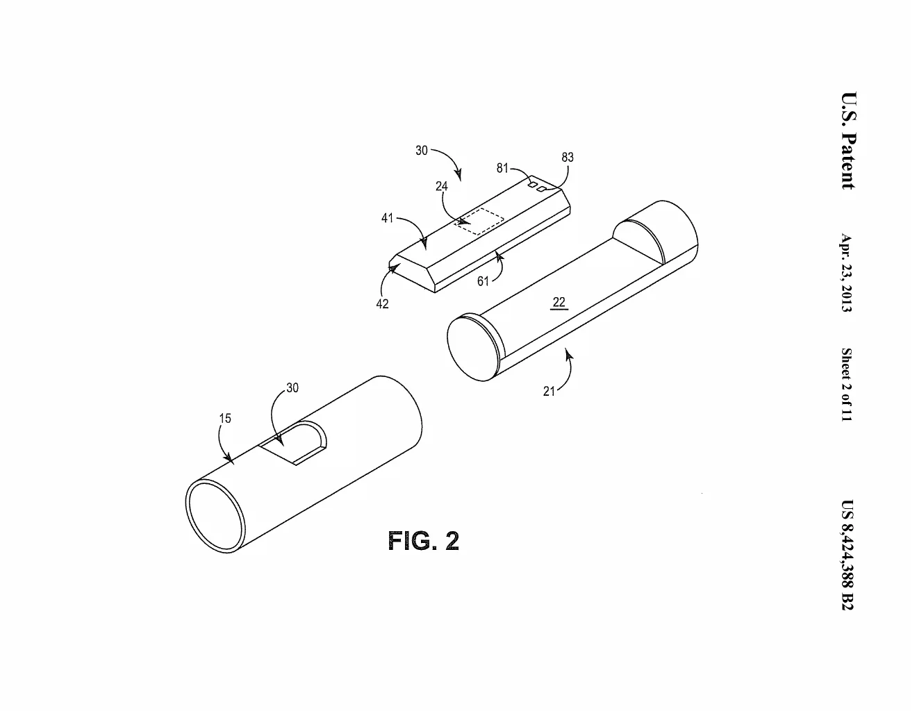
US 8,424,388 · from the drawings An exploded view of the pressure-sensor module and the tubular housing halves that carry it inside an implantable lead. -
US 8,433,402 Hermetic Packaging & Feedthroughs Hermetic wafer-to-wafer bonding with electrical interconnection
Building an implantable device from two bonded silicon wafers means the join has to do two jobs at once: carry electrical signals between the wafers AND seal the electronics hermetically against body fluid. This patent makes a single heated step do both — conductive pads set into vias on each wafer reflow, agglomerate, and merge, so the electrical interconnect IS the hermetic seal. One operation replaces two, at wafer scale.
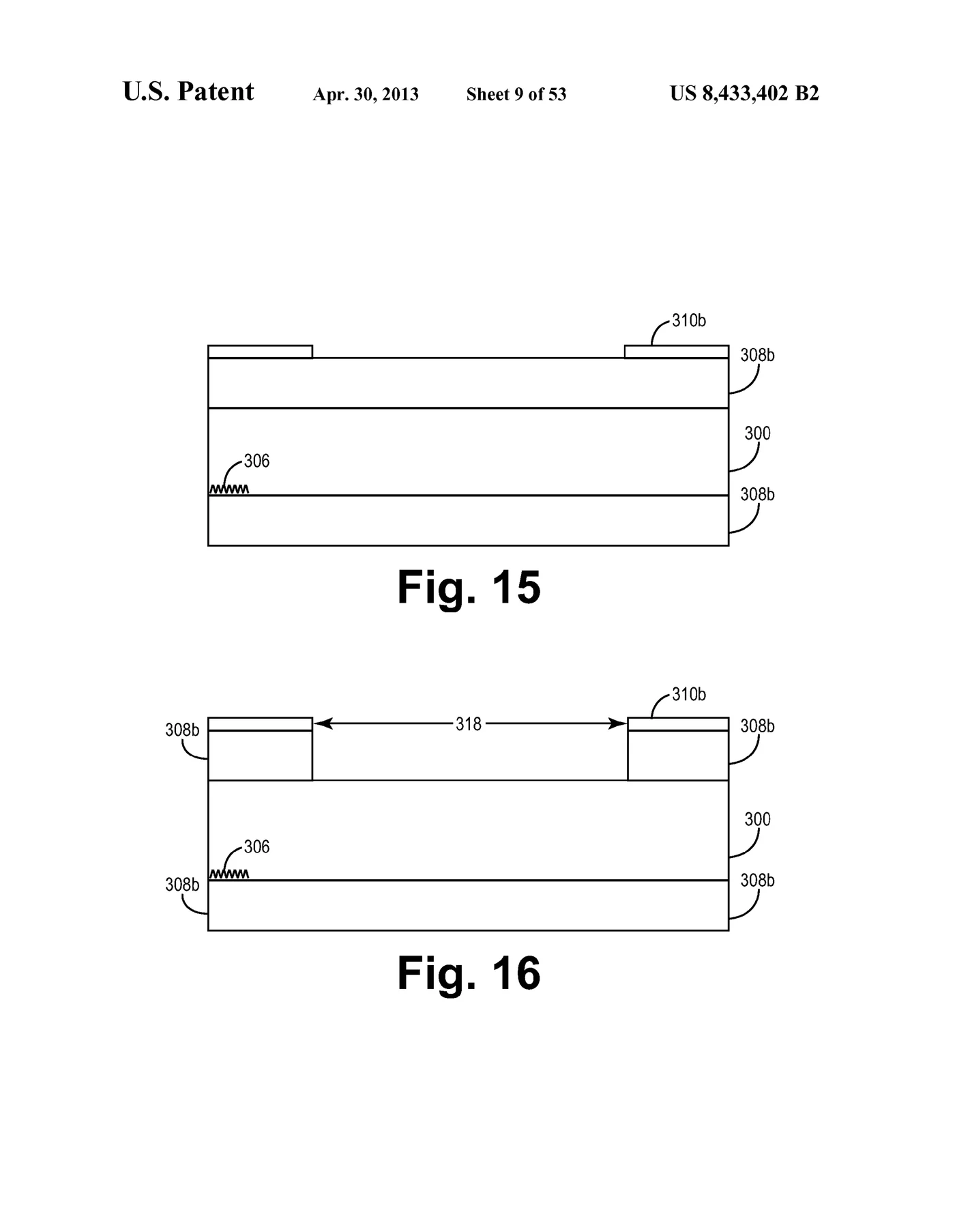
US 8,433,402 · from the drawings Cross-sections of the stacked wafers: recessed conductive pads on each face that, when heated, reflow and merge — forming the electrical interconnect and the hermetic seal in the same step. -
US 8,461,681 Interconnects & Materials Layered structure for corrosion resistant interconnect contacts
Electrical contacts that sit in blood corrode, slowly degrading an implanted sensor over the years it must survive. This sole-inventor design armors them in a three-layer sandwich — titanium-niobium, niobium, titanium-niobium again — chosen for corrosion resistance and for thermal expansion that can be tuned to match the silicon beneath. It was filed the same day as its twin, the negative-expansion weld pad, as two complementary answers to the slow thermal-mechanical death of interconnects.
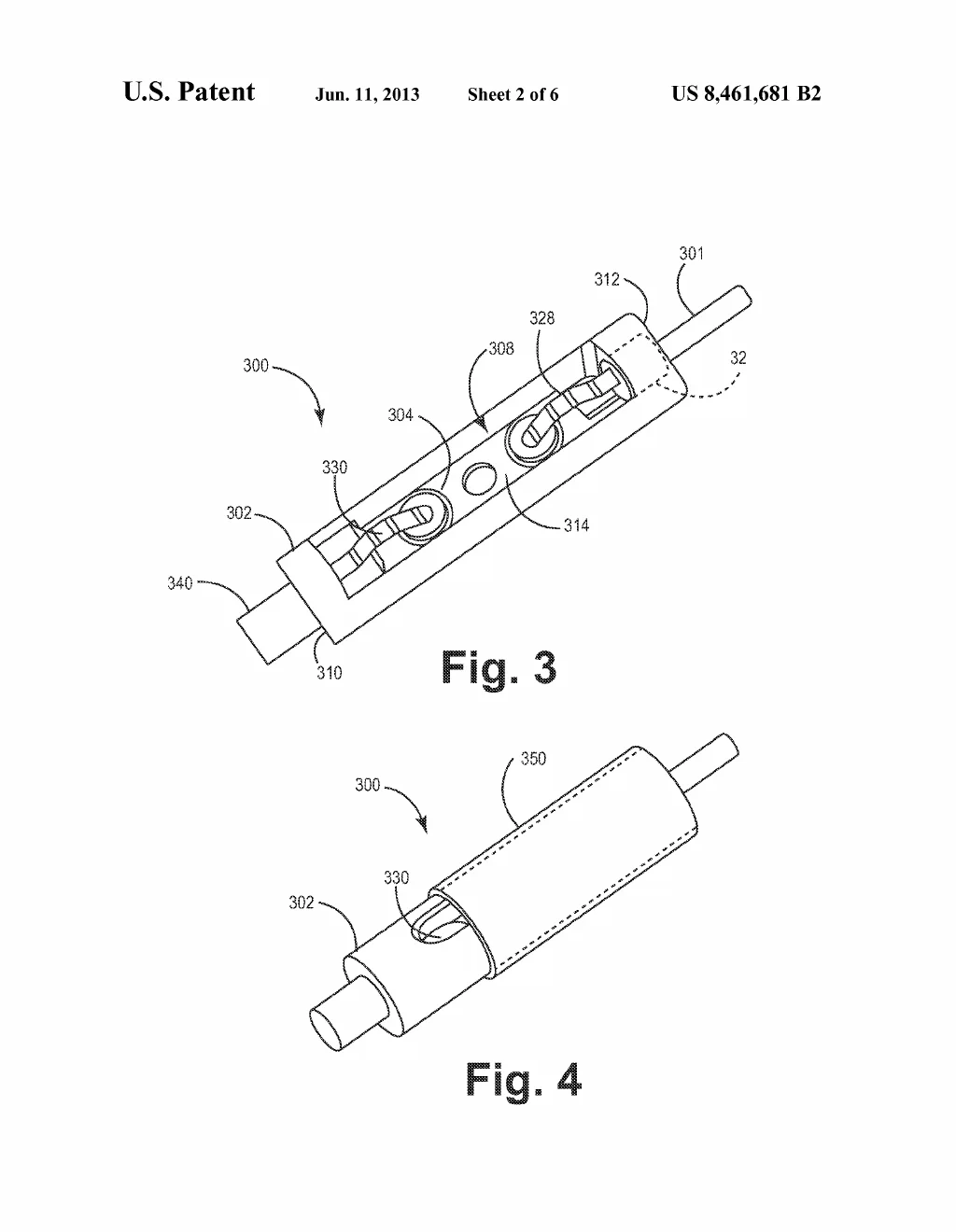
US 8,461,681 · from the drawings A cutaway perspective of the sensor capsule built into an implantable lead, exposing the interconnect contacts the layered coating is designed to protect. -
2014 US 8,666,505 Power Sources Wafer-scale package including power source
Direct wafer bonding runs hot enough to destroy a battery — yet a device isn't truly complete at wafer scale until its power source is sealed inside. This design puts the control chip and the battery together in a cavity between two bonded substrates, then closes the seam with low-temperature laser-assisted bonding so nothing inside is harmed. It became one of the most-cited pieces of work in the corpus, with 126 later patent families drawing on it as tiny self-powered leadless implants became an industry.
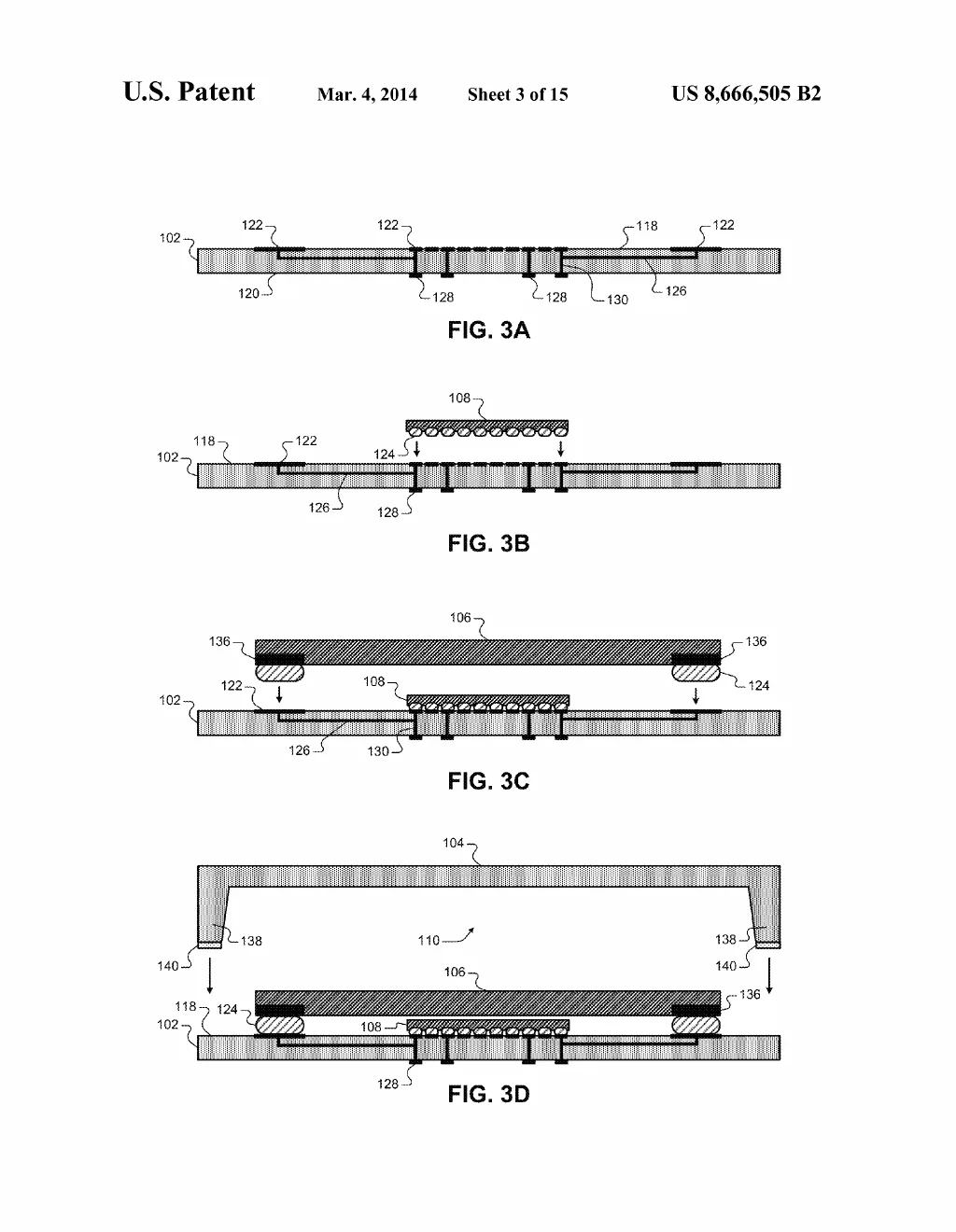
US 8,666,505 · from the drawings Four cross-section stills of the build: the wired base, the chip soldered on, the flat battery lowered onto its pads, and the recessed lid descending to seal both inside one cavity. -
US 8,796,109 Laser Materials Processing Techniques for bonding substrates using an intermediate layer
Some pairs of materials simply refuse to bond directly, and heating a whole stack would wreck whatever is inside. The trick here is a film just tens of nanometers thick sandwiched between the two surfaces: laser light passes clean through the top substrate and heats only that film, welding the pair right at the seam. There is even built-in quality control — the tinted film turns optically clear where the bond succeeds, so a good seal can be inspected by eye.
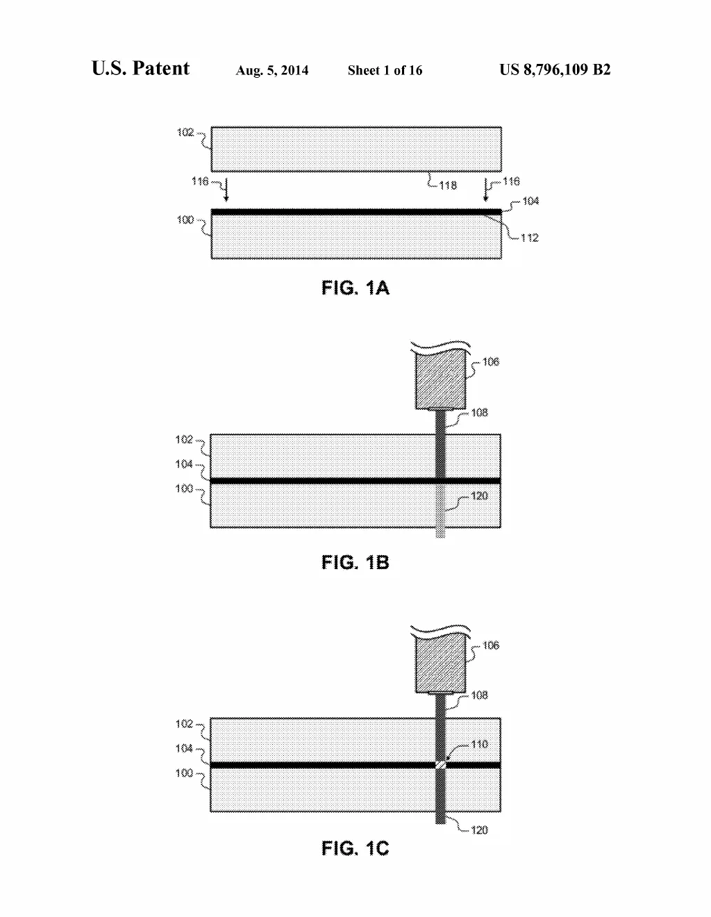
US 8,796,109 · from the drawings Three cross-section steps showing two substrates brought together over a nanometers-thin film, then fused where a laser shining through the top layer heats the film. -
2015 US 9,120,287 Laser Materials Processing Techniques for Bonding Substrates Using an Intermediate Layer
Joining two solid wafers, such as glass or silicon, without cooking the whole assembly is hard: broad heating warps parts and destroys delicate circuitry sealed inside. This method lays down a thin absorbing film between the two pieces and fires a laser straight through the transparent top substrate, so only the buried film heats up and welds the parts together exactly where the beam lands. It creates a strong, hermetic seal at room temperature everywhere else, protecting sensitive electronics inside implantable devices.
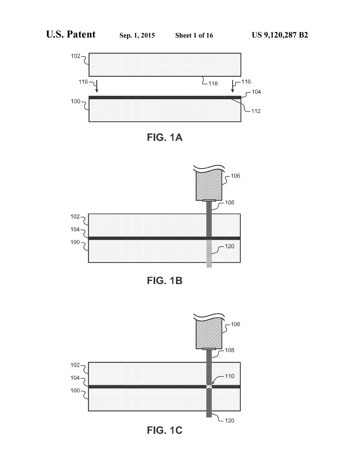
US 9,120,287 · from the drawings Cross-section of two stacked substrates with a thin intermediate layer between them, showing a focused laser beam passing down through the top substrate to fuse the layer at a localized bond spot. -
US 9,171,721 Laser Materials Processing Laser assisted direct bonding
Conventional direct bonding fuses two polished parts by heating them past 400°C in bulk — and that heat warps and cracks the very joint it is meant to strengthen, especially between mismatched materials. This method simply presses the parts into contact to form a weak room-temperature bond, then traces a laser along the seam to strengthen it locally while everything else stays cool. It is the keystone of the corpus's laser craft — the bridge between generic direct bonding and the whole family of laser-bonded packages that followed.
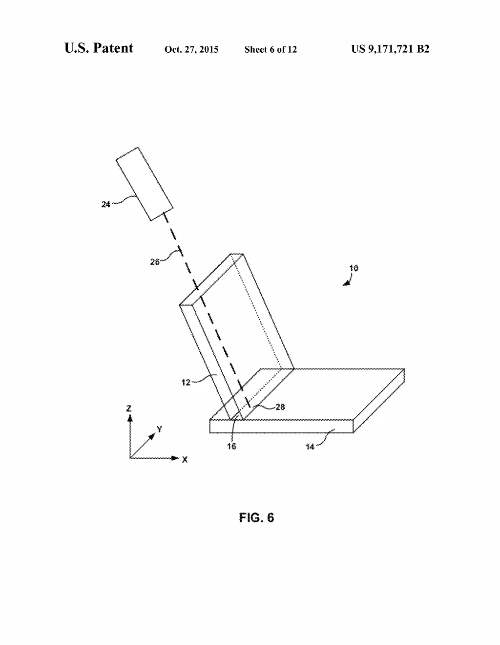
US 9,171,721 · from the drawings A laser aimed through the tilted transparent plate at the seam where it meets the base wafer, strengthening the bond where the two touch. -
2016 US 9,252,415 Power Sources Power sources suitable for use in implantable medical devices and corresponding fabrication methods
A single thin-film battery cell is only about 14 microns thick — far too little energy on its own to power an implant. So the cells are made like chips, in arrays on wafers, then stacked: routing layers carry each cell's contacts out to the side, vias gang the aligned contacts in parallel, and micron-scale cavities engineered between the cells give them room to swell as they charge. IBM and France's atomic-energy agency are among the citing parties — battery stacking with relevance well beyond medicine.
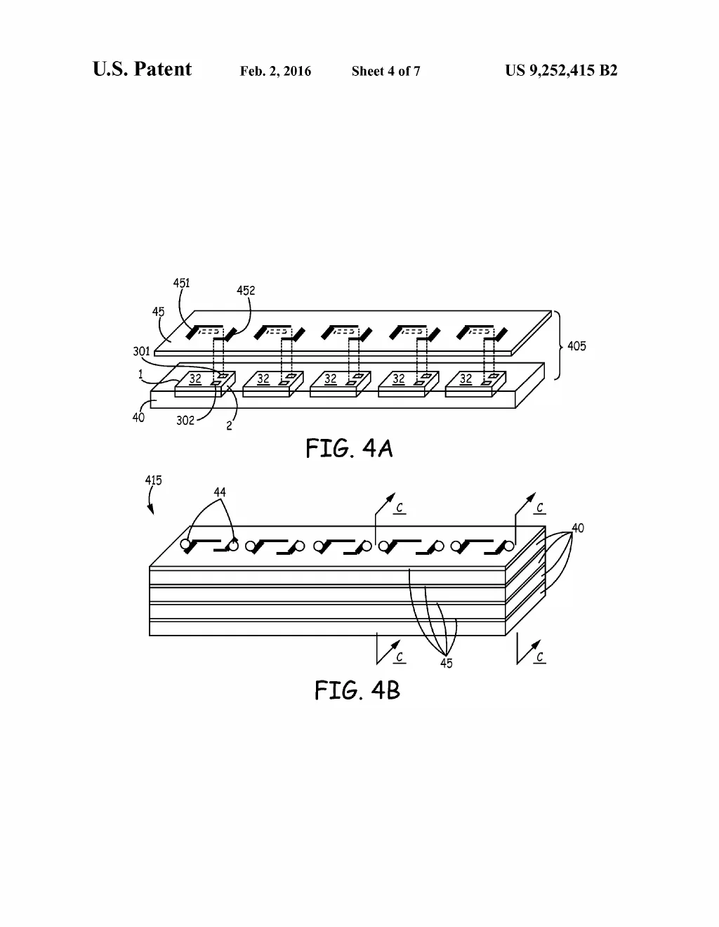
US 9,252,415 · from the drawings Battery cells arrayed on a wafer with the routing layer hovering above them, and the finished multi-layer stack they become. -
US 9,318,400 Power Sources Wafer-scale package including power source
Fusing two wafers into one sealed package normally takes 400°C or more — heat that would destroy any battery inside — yet a device is not truly wafer-scale-complete without its power source built in. This design encloses both the control chip and its battery in a cavity between two bonded substrates, hermetically sealed by low-temperature laser-assisted bonding, and explicitly contemplates leadless device configurations. With 151 later patent families citing it, it is the most-cited grant in the corpus.
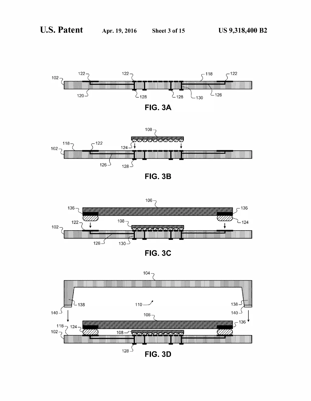
US 9,318,400 · from the drawings Four-step assembly sequence: a wired glass wafer, the chip lowered on, the battery lowered on, and a second wafer descending to seal both inside. -
US 9,431,312 Power Sources Wafer-Scale Package Including Power Source
An implantable medical device has to be tiny, sealed tight against the body, and carry its own power — usually meaning a bulky separate battery and housing. This design instead builds the whole thing at wafer scale: a control chip and a thin-film energy-storage device are mounted on one substrate, then a second substrate is bonded over them to seal both inside a single hermetic cavity. The result is a self-powered sensing-and-stimulation package small enough to go where earlier electronics-plus-battery assemblies could not.
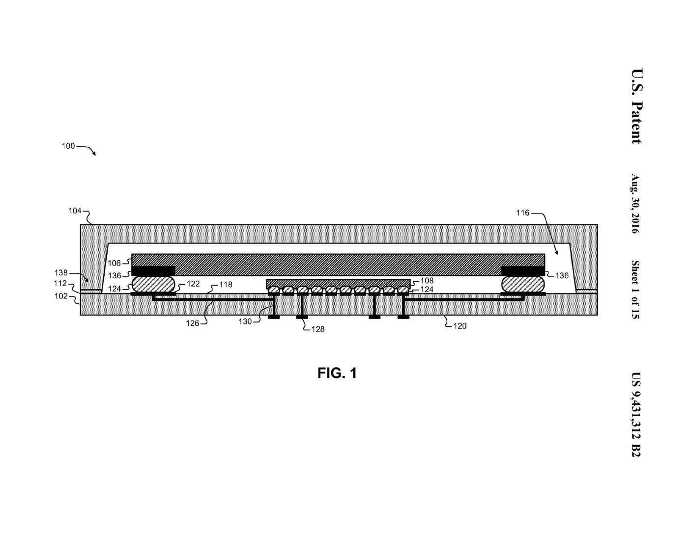
US 9,431,312 · from the drawings Cross-sectional view (FIG. 1) of the wafer-scale package: two bonded substrates form a sealed cavity holding both the control-module die and the energy-storage device that powers it, with conductive vias and traces routing signals through the walls. -
2017 US 9,616,223 Implantable Sensors Media-exposed interconnects for transducers
Some sensor connections cannot hide behind a hermetic wall — the strain of a beating heart is too much for sealed designs — yet bare connections corrode. This one stacks two conductive layers whose stresses pull in opposite directions, one compressive and one tensile, cancelling to almost no net load, and builds the contacts from valve metals like titanium whose surface oxide resists corrosion in saline. Filed in 2005 and granted twelve years later, it is cited by Endotronix, the company behind an implantable heart-failure pressure sensor.
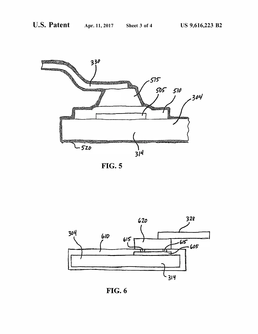
US 9,616,223 · from the drawings Cross-section of the exposed connection: layered metal draped over the sensor contact, built to face body fluids directly. -
US 9,688,053 Laser Materials Processing Devices Formed With Techniques for Bonding Substrates Using an Intermediate Layer
Sealing two rigid plates of glass or similar material together usually means heating the whole assembly, which can warp the parts or damage anything delicate inside. This device is bonded by laying down a thin absorbing film between the two plates and firing a laser through the top plate so only that film heats up, fusing the plates precisely where the beam lands while everything around it stays cool. The result is a strong, hermetic seal that can enclose sensitive electronics without cooking them.
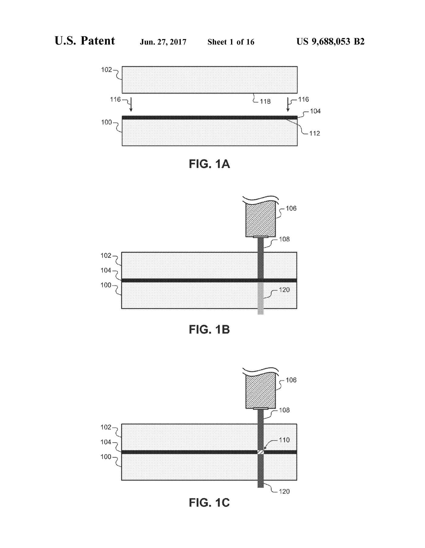
US 9,688,053 · from the drawings Cross-section (FIGS. 1A-1C) showing a laser directing a focused beam down through the transparent top substrate onto a thin intermediate layer, which absorbs the energy and fuses the two substrates together at that spot. -
US 9,832,867 Hermetic Packaging & Feedthroughs Embedded metallic structures in glass
Implant packages have to keep shrinking without giving up their airtight seal, and wiring that lives only on the surface wastes the walls. Here two glass wafers are fused with filled vias, conductive traces, and an insulating layer between them, turning the glass itself into three-dimensional wiring — even an antenna can be etched straight into the wafer, so the wall becomes a working radio component instead of mere enclosure. The interconnect industry noticed: four of the five visible follow-on citations come from connector maker Samtec.
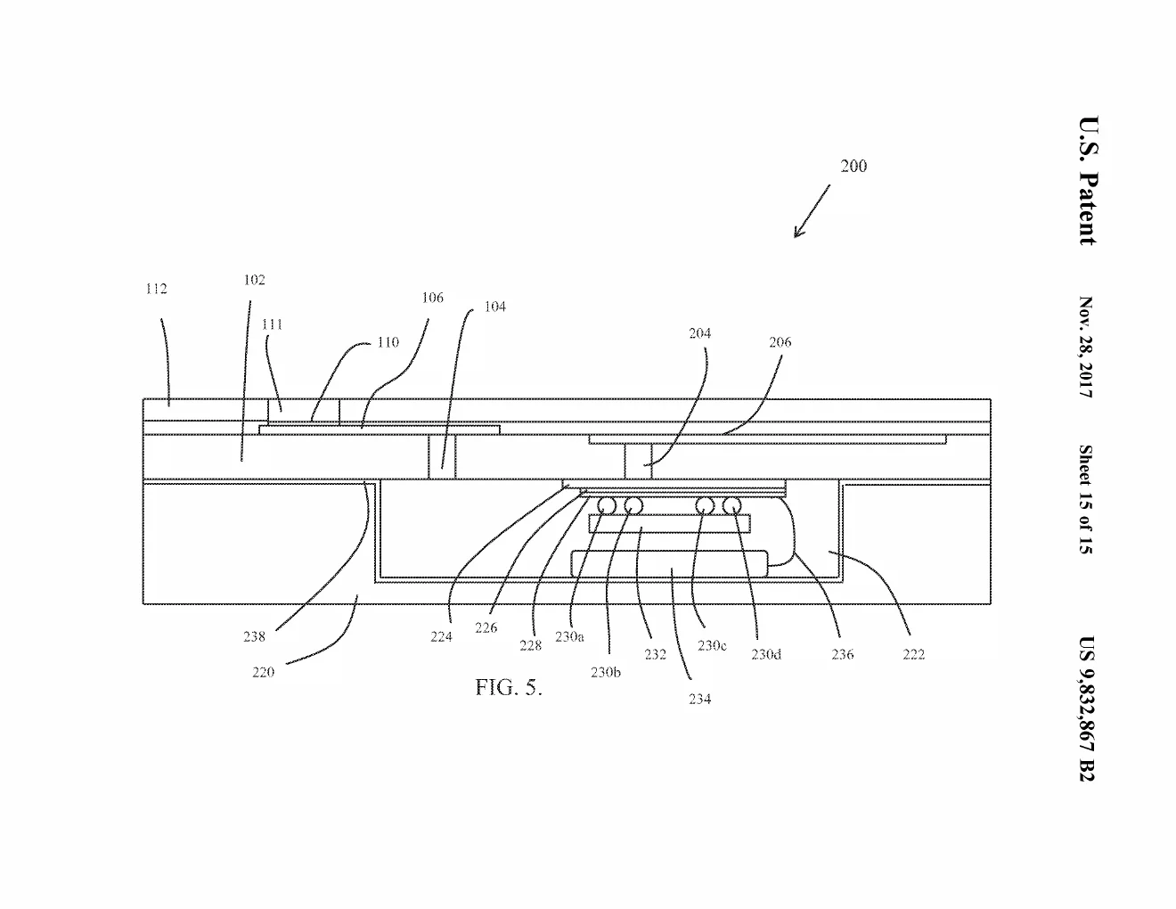
US 9,832,867 · from the drawings Cross-section of the finished package: two glass wafers fused into one body, with a chip mounted inside and metal routing buried in the glass wall itself. -
2018 US 9,865,533 Hermetic Packaging & Feedthroughs Feedthrough assemblies (parent of the laser-bond feedthrough line)
Every implantable device faces the same paradox: its electronics must be sealed away from body fluid absolutely, yet wires have to pass through the wall. This grant founded his answer — instead of baking glass and metal together at furnace temperatures, a laser traces a ring-shaped bond around each wire's passage, fusing it shut while the rest of the part stays cool. It grew from a provisional application filed on Christmas Eve 2014 and seeded a decade-long line of patents.
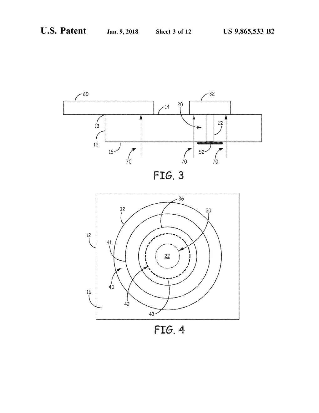
US 9,865,533 · from the drawings Laser beams fire up through the transparent substrate to weld a contact in place, beside a bullseye view of the ring-shaped bond encircling the wire's via. -
US 9,913,693 Flow Control & Surgical Navigation Error correction techniques in surgical navigation
Magnetic tracking pinpoints a surgical instrument faster than the patient can be re-imaged, so every heartbeat and breath shifts the anatomy and leaves the instrument drawn in the wrong place on a frozen picture. The fix pairs the magnetic sensor with an accelerometer: when acceleration spikes, the system falls back on trusted earlier positions, and frequency analysis can even tell a heartbeat from a breath from the surgeon's own hand. It is his accelerometer craft resurfacing thirteen years later in the operating room, now cited by 145 later patent families.
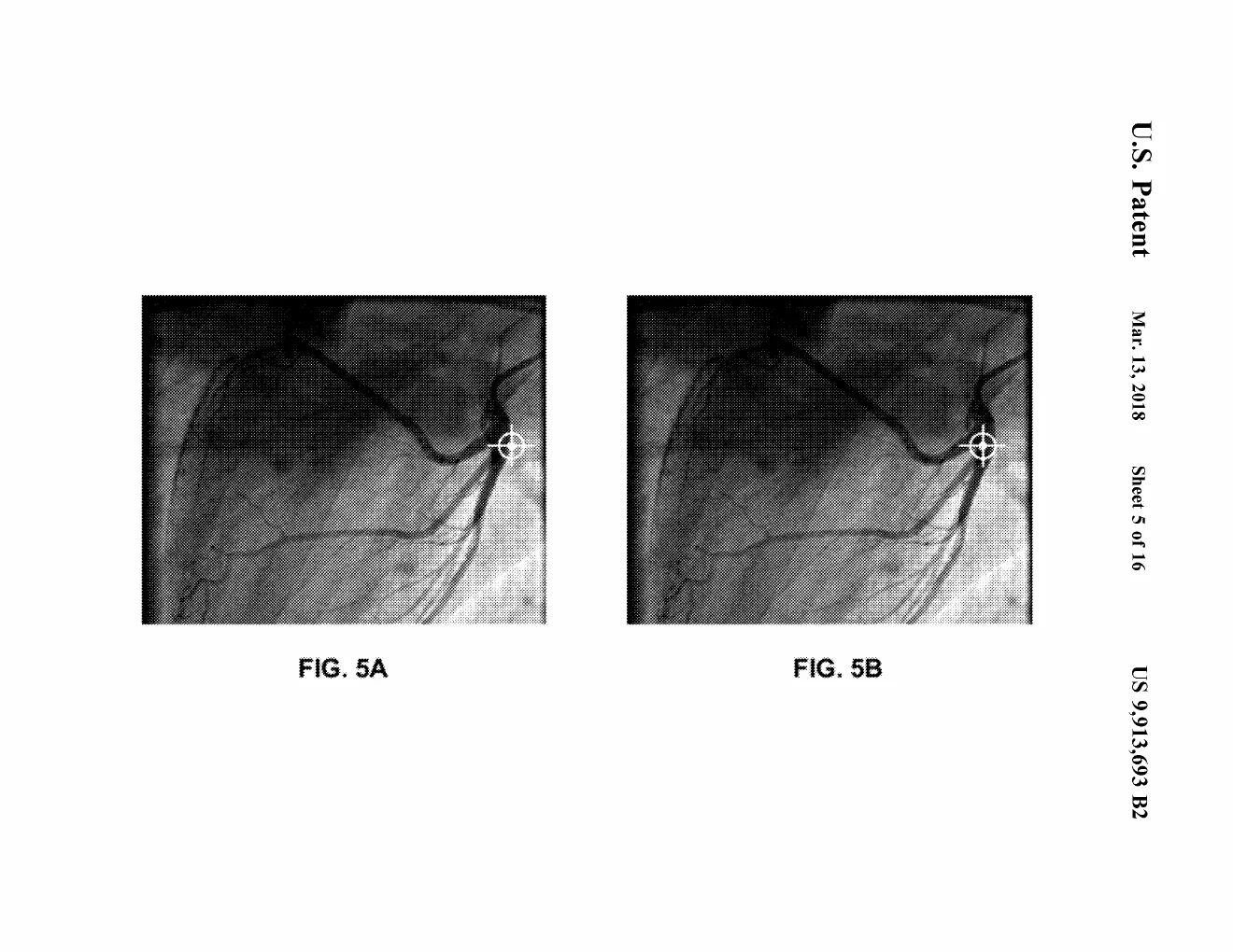
US 9,913,693 · from the drawings Two angiogram images from the patent itself, a crosshair marking the tracked instrument's position on the heart. -
US 10,096,393 Power Sources Nuclear radiation particle power converter
A betavoltaic cell works like a solar panel lit by radiation instead of sunlight — but a flat panel lets much of each particle's energy slip away before it is collected. This design crumples the collector into a three-dimensional sponge of coated nanostructures, so nearly every particle strikes a working junction before its charge can fade. It founded the patent line reconnecting Medtronic to its nuclear-pacemaker heritage: the pursuit of an implant whose power source never needs replacing.
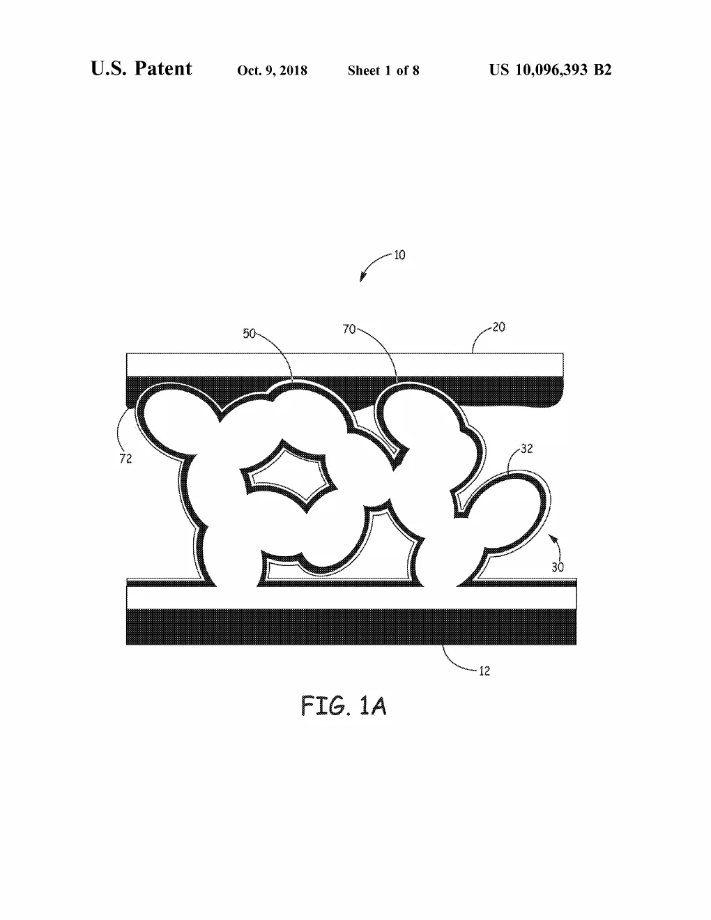
US 10,096,393 · from the drawings Cross-section of the betavoltaic cell: a sponge-like tangle of coated nanostructures filling the gap between two flat electrode plates. -
US 10,124,559 Laser Materials Processing Kinetically limited nano-scale diffusion bond structures and methods
Joining sapphire to titanium — a transparent gem to an opaque metal — normally demands a furnace at 600 to 1000 °C. Invented with Corning, this technique fires a laser through the sapphire so its energy lands only at the buried interface, in a flash too brief for the heat to wander, leaving a bond thinner than 1000 nanometers between two materials that never felt an oven. The Corning co-assignment is the corpus's clearest external validation: a materials-science giant putting its name beside his.
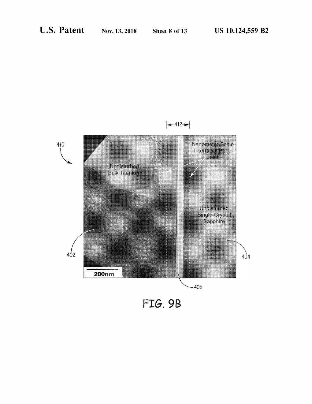
US 10,124,559 · from the drawings A real electron-microscope image: undisturbed titanium on one side, undisturbed single-crystal sapphire on the other, and a bond joint only nanometers wide running between them. -
2019 US 10,420,509 Hermetic Packaging & Feedthroughs Sealed package and method of forming same
Conventional hermetic housings hang their fate on feedthroughs built from ferrules, glass seals, and high-temperature brazing — complexity and stress concentrated at the one joint an implant cannot afford to lose. This grant, part of a four-patent chain with Craig L. Schmidt, continues the sealed-package alternative: a cavity in the substrate covered to form the enclosure, with each external contact laser-bonded in a ring around its via, heating only a whisper-thin surface layer.
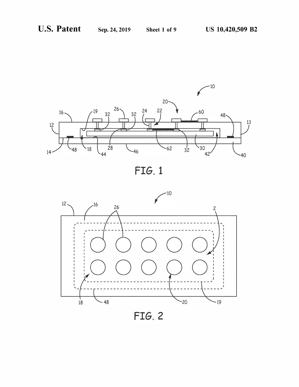
US 10,420,509 · from the drawings A side cross-section of the sealed package — cavity, cover, and capped vias — above a top view of its grid of ten round external contacts. -
US 10,464,836 Hermetic Packaging & Feedthroughs Hermetic conductive feedthroughs for a semiconductor wafer
How do you carry a signal out through a glass wall without giving body fluid a path back in? Here the conductor is entombed in the wafer itself — its outer face never reaches the surface directly, but takes a deliberate dog-leg through an embedded trace to a recessed cavity, so fluid can never follow the interface back inside. Filed in 2013, it founded the glass-wafer feedthrough line for making implants at wafer scale.
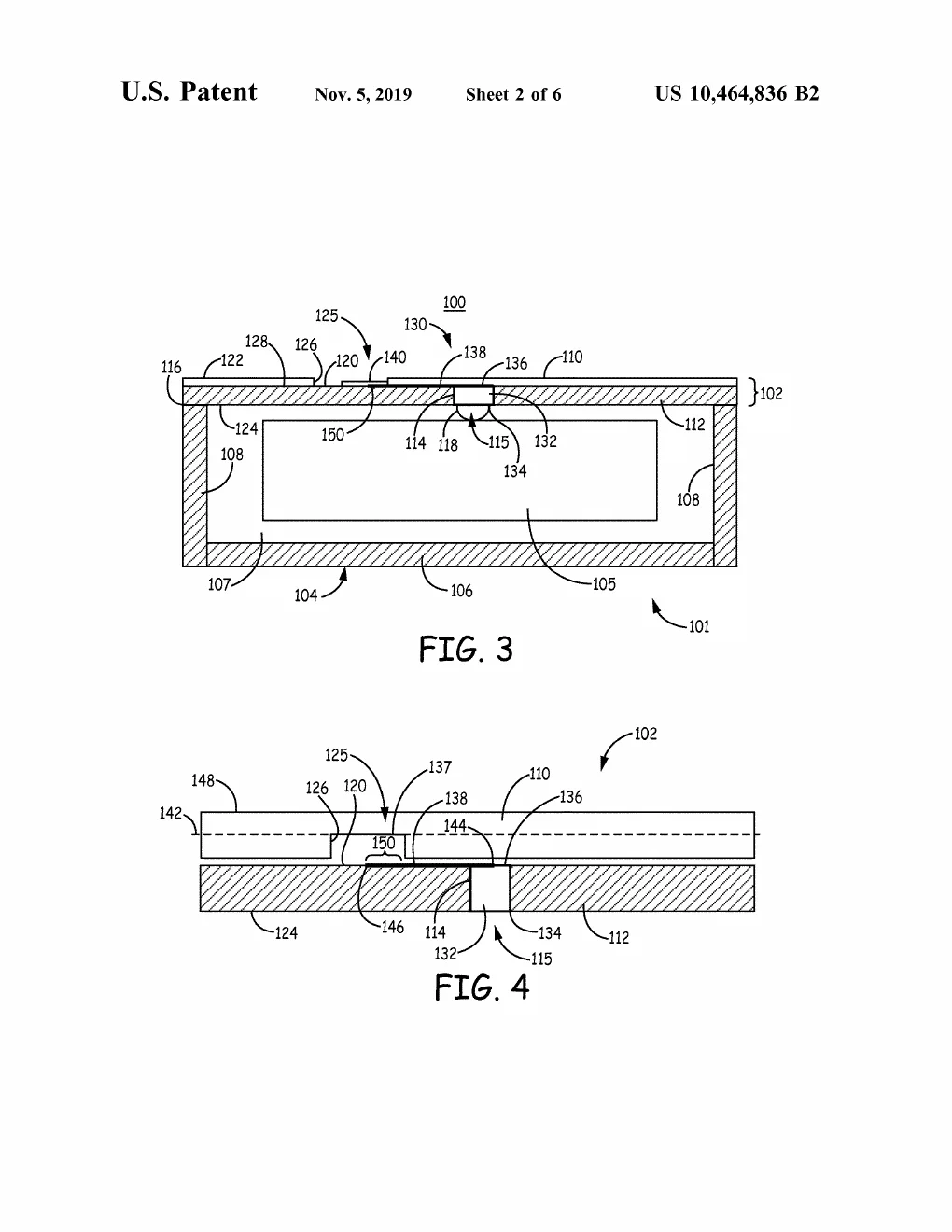
US 10,464,836 · from the drawings A cross-section of the implantable device with the feedthrough in its wall, and a close-up showing the conductor buried inside the glass rather than crossing straight through.
2020s
The frontier: MEMS flow control for hydrocephalus, betavoltaic refinements, and sealed packages granted into 2026 — the line still running.
24 grants
-
2020 US 10,535,596 Hermetic Packaging & Feedthroughs Feedthrough assemblies and methods of forming same
This is the core articulation of the laser-bond feedthrough claim: a conductive via passes through a non-conductive substrate, and the contact capping it is hermetically sealed by a bond that surrounds the via — an interface that can be just tens of nanometers thin. Because the light delivers heat only where the joint forms, the wall can be glass, sapphire, or even silicon carbide, and the device can shrink without ever compromising the seal.
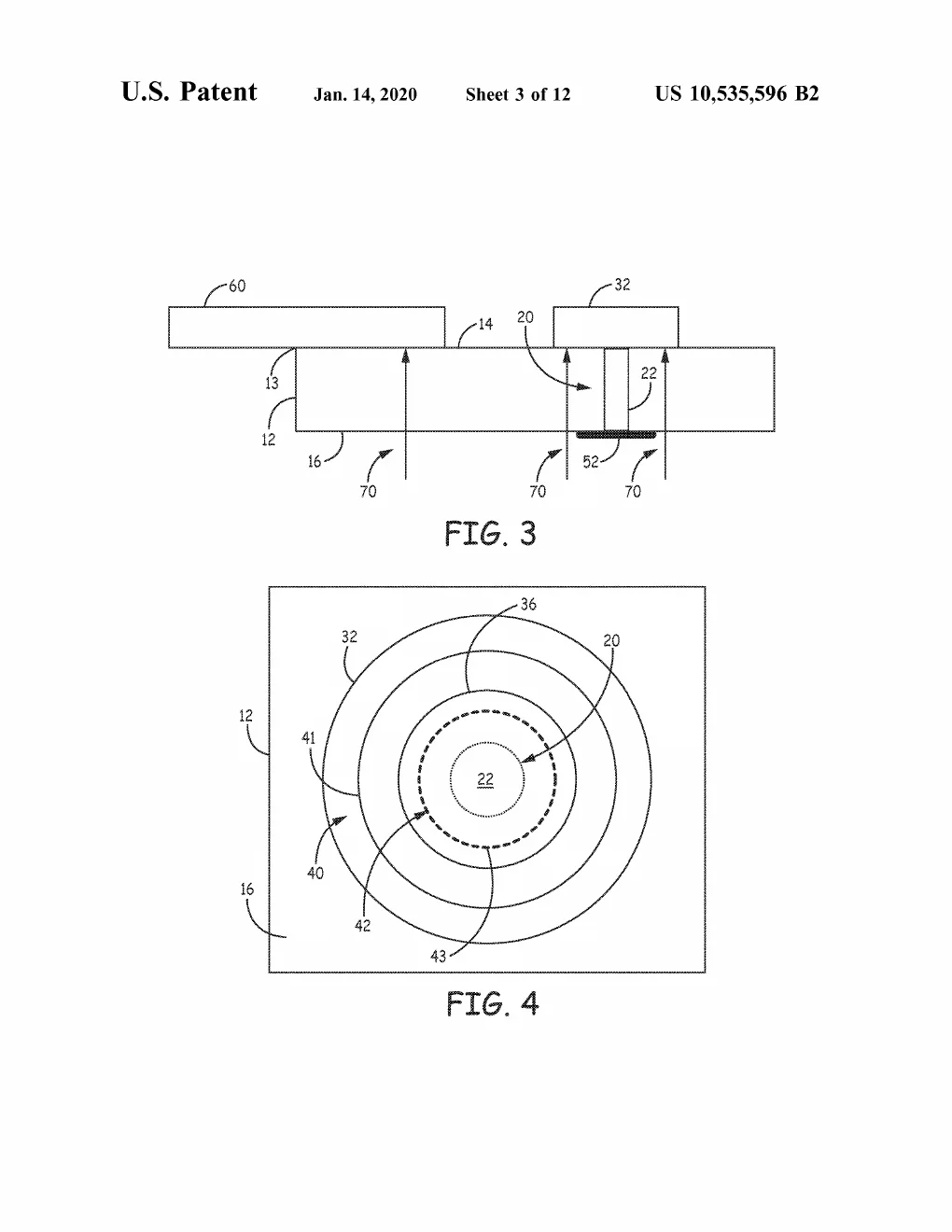
US 10,535,596 · from the drawings A cross-section catches the laser mid-weld, firing through the see-through substrate, with a plan view of the concentric ring-shaped bond zones around the wire. -
US 10,765,372 Hermetic Packaging & Feedthroughs Sealed package and method of forming same
In this continuation of the sealed-package line with Craig L. Schmidt, the package stops being a box that contains the device and becomes the device's own body: a cavity carved into the substrate, a cover layer sealing it shut, and a via carrying signals out to a contact laser-bonded in a ring around it. The laser heats only the surface layer where the joint forms — and the finished bond is stronger than the bulk substrate around it.
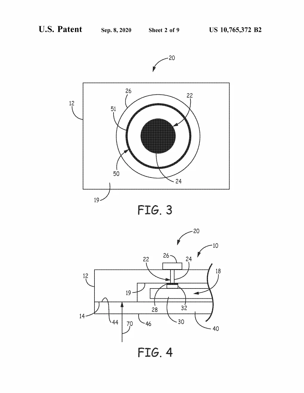
US 10,765,372 · from the drawings A bullseye view of one external contact with its ring-shaped bond, and a close-up cross-section showing the contact's via reaching down into the sealed cavity. -
US 10,811,157 Power Sources Nuclear radiation particle power converter
A flat radiation-to-electricity converter wastes much of what its fuel emits: charge carriers recombine before they can be collected. This continuation carries the 3D answer forward — a sponge-like collector of nanorods, nanotubes, or foam, coated with charge-separating layers such as quantum dots, with the isotope infiltrated into the structure itself, even by exposing the finished sponge to pressurized tritium gas. It is a solar cell rebuilt around beta decay, with the fuel soaked into the electrode.
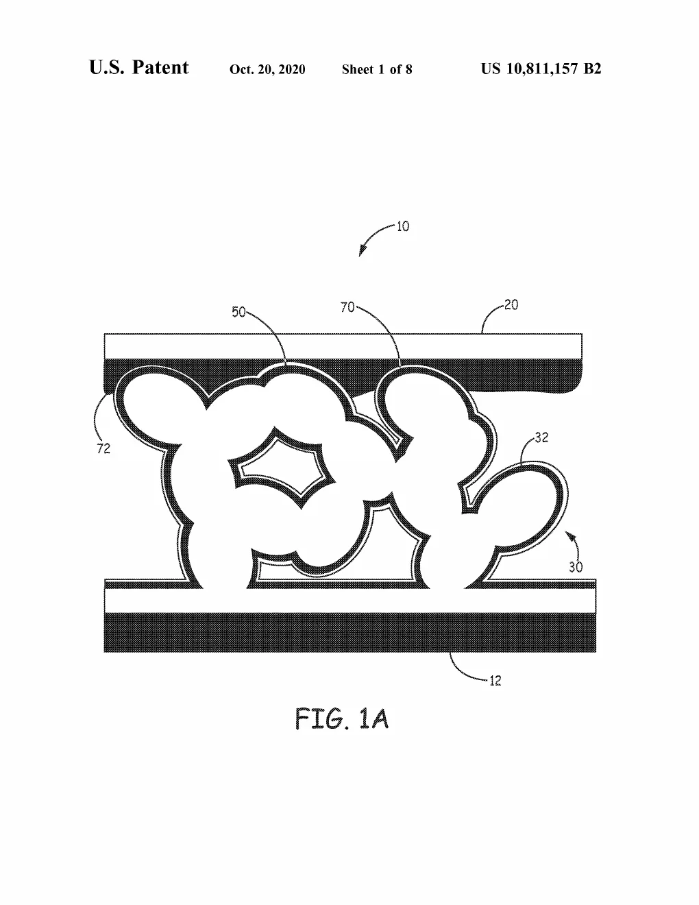
US 10,811,157 · from the drawings A cross-section of the sponge-like 3D collector — a tangle of coated nanostructures filling the gap between two flat electrode plates. -
US 10,813,238 Hermetic Packaging & Feedthroughs Hermetically-sealed packages including feedthrough assemblies
Where its sibling grants claim the feedthrough alone, this sole-inventor patent claims the whole sealed package built around it: the substrate carrying the laser-bonded contacts is integrated into the device's hermetic housing itself. It descends from one of the twin provisional applications filed on Christmas Eve 2014 — the branch of the feedthrough line he pursued under his name alone.
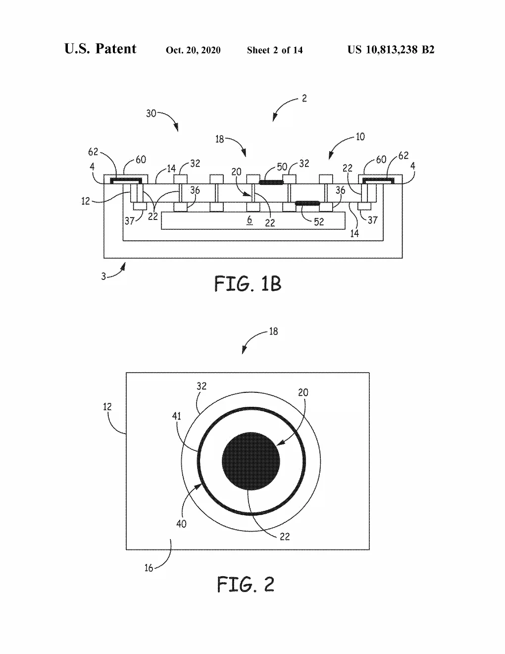
US 10,813,238 · from the drawings A cross-section of the sealed package with its feedthrough contacts, paired with a top-down view of one contact — the dark via at center ringed by its bond. -
US 10,818,811 Power Sources Power source and method of forming same (radioluminescent: radioactive to light to photovoltaic)
Instead of converting radiation straight to electricity, this power source takes a detour through light: a hermetically sealed cavity holds radioactive material beside a phosphor that glows under its particles, and a photovoltaic layer harvests the glow. The design even accounts for the helium that tritium decay produces, using a gas-permeable substrate so the sealed cavity doesn't slowly pressurize itself over the decades — a battery designed around its own exhaust. It founded the radioluminescent branch of the corpus's nuclear-power line.
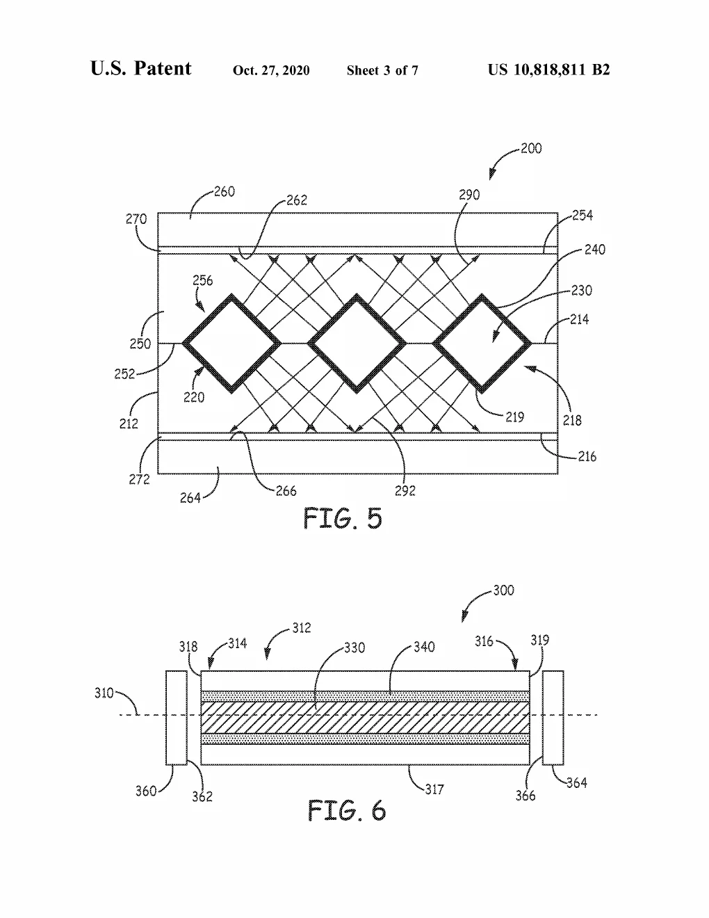
US 10,818,811 · from the drawings A cross-section mid-glow: rays of light criss-cross from the embedded particles to the energy-harvesting layers above and below. -
2021 US 10,981,355 Laser Materials Processing Kinetically limited nano-scale diffusion bond structures and methods
A laser pulse fired through sapphire deposits its energy exactly at the interface with the metal beneath, forming a diffusion bond thinner than a thousand nanometers. 'Kinetically limited' is the heart of it: the flash is too brief for heat to migrate, so diffusion happens only in that nano-zone and the parts never really get hot — with named applications reaching past medical packaging to vacuum windows, photonics, and spacecraft. The patent carries both Medtronic's and Corning's names — a materials-science giant's endorsement written into the record.
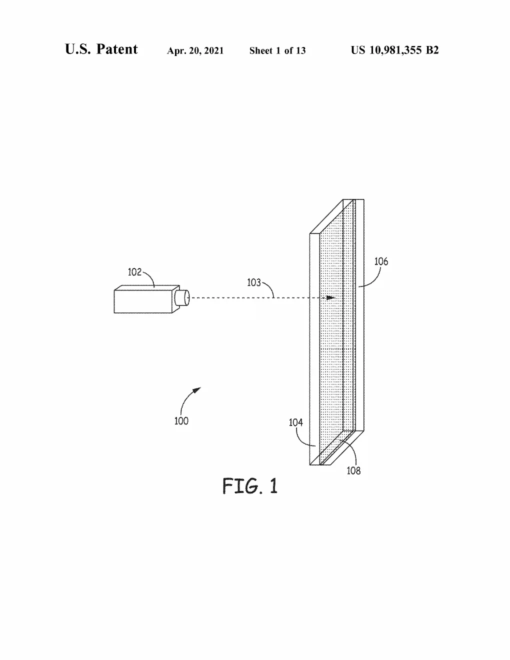
US 10,981,355 · from the drawings A laser fires its beam through a transparent sapphire sheet stacked against a metal plate, landing its energy at the hidden interface where the bond will form. -
US 11,103,714 Hermetic Packaging & Feedthroughs Sealed implantable medical device and method of forming same
Feedthroughs are where hermetic seals leak, and high-temperature joining can alter the very materials it connects. This axial design sidesteps both: the external contact is sealed at one end of the housing, and electricity crosses to the electronics inside through a conductive member held under compression — connection by pressure, not bonding. The housing can even be transparent glass or sapphire, letting an optical sensor read the body straight through the wall with no extra opening.
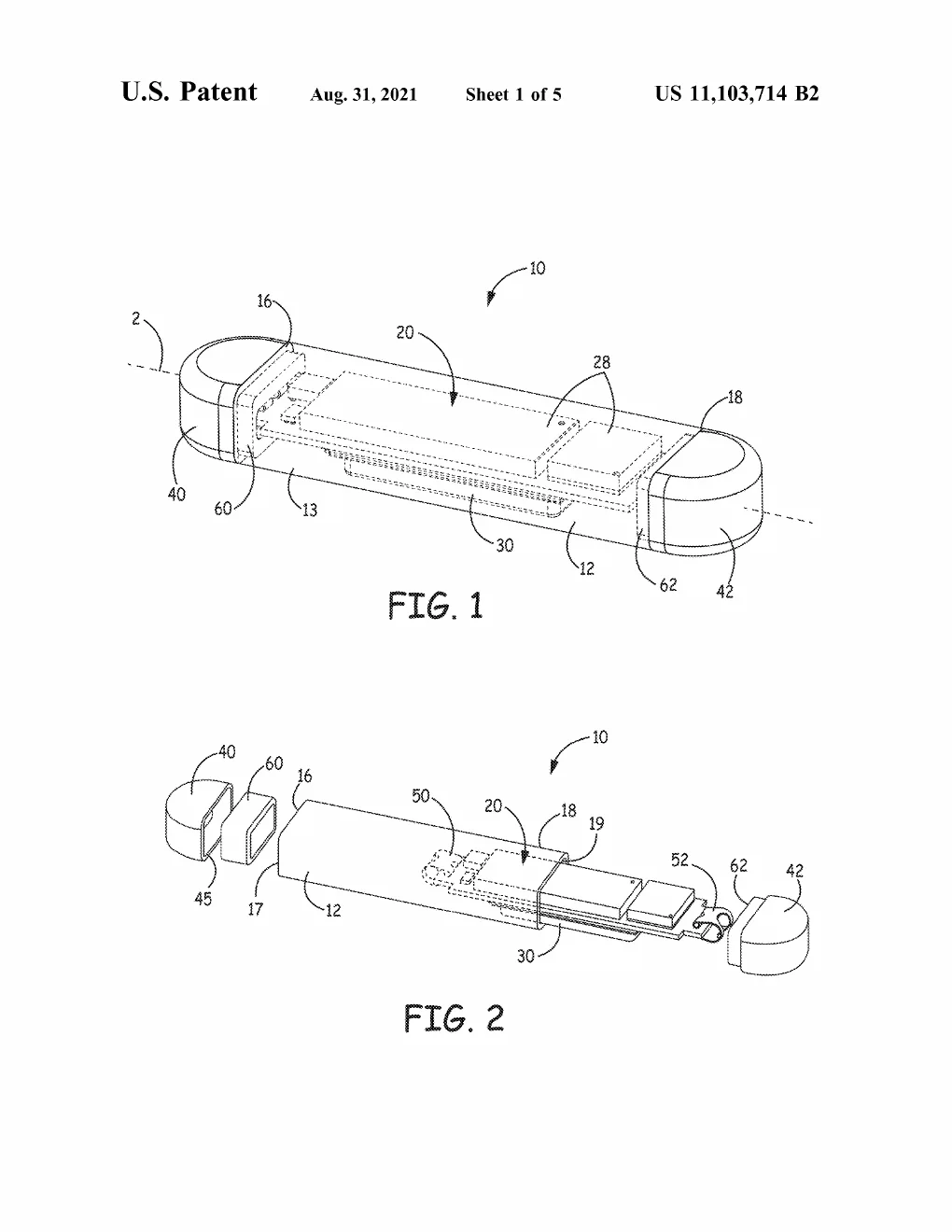
US 11,103,714 · from the drawings The capsule-shaped device seen whole and pulled apart along its axis — end caps, seal rings, and the electronics that slide into the tube. -
US 11,189,390 Power Sources Power source and method of forming same
A nuclear battery is only as good as its fuel storage, and tritium — a workhorse isotope — is a gas, which limits how much power can be packed into a small space. The answer here is a loaded substrate: a carrier material holds the isotope densely, thin deposited barrier layers keep it from wandering, and the whole assembly sits inside a sealed enclosure. Contain the fuel properly, and the rest of the battery can do its job.
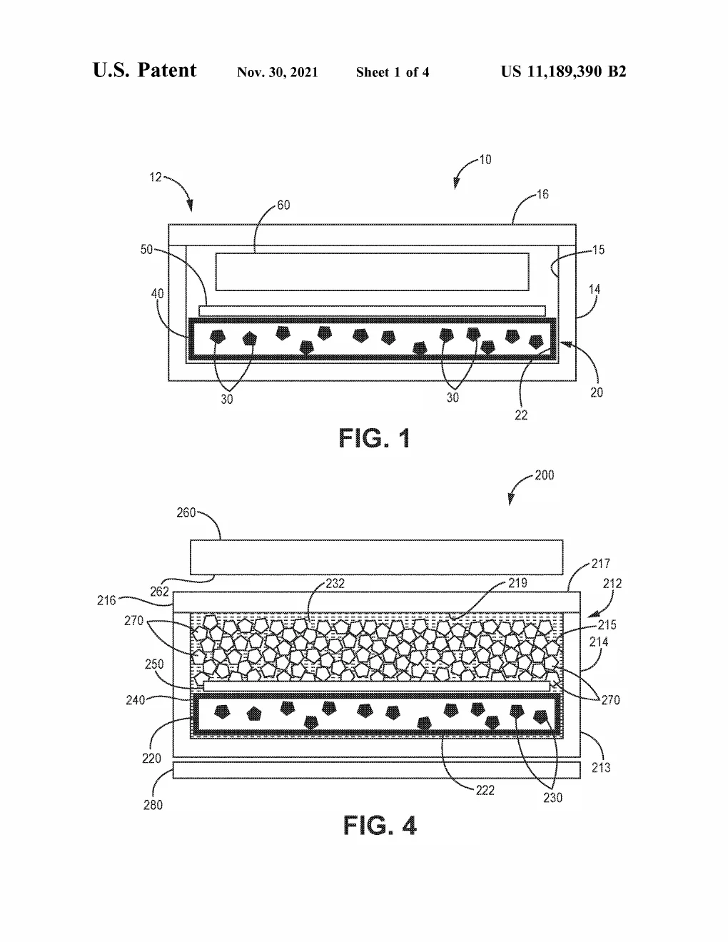
US 11,189,390 · from the drawings Cross-sections of the sealed power source: the isotope-bearing layer at the floor of its housing, and a variant packed with granular carrier material beneath the cover. -
2022 US 11,419,552 Hermetic Packaging & Feedthroughs Sealed package and method of forming same
Traditional hermetic feedthroughs are little assemblies of ferrules, glass seals, and high-temperature brazing — manufacturing complexity and material stress at the most critical joint in the device. This continuation refines the alternative: a substrate with a sealed cavity that is itself the device body, each electrical contact laser-bonded in a ring around its via. The laser heats only the surface layer it touches, and the finished bond is stronger than the bulk of the substrate around it.
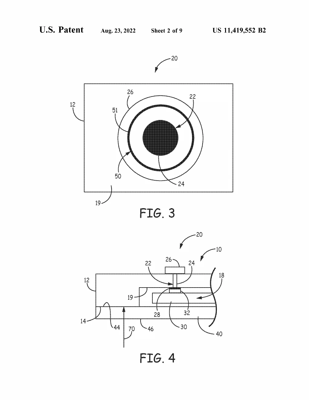
US 11,419,552 · from the drawings A bullseye top view of one contact ringed by its bond line, above a close-up cross-section with laser energy firing up through the substrate to weld it in place. -
US 11,485,670 Hermetic Packaging & Feedthroughs Hermetic conductive feedthroughs for a semiconductor wafer
As implants shrink, the wired doorways through their walls have to shrink too — and conventional feedthrough builds don't miniaturize reliably. Here the conductor is entombed inside a glass wafer, its outer face never reaching the surface directly: the path out takes a deliberate dog-leg through a buried trace to a recessed cavity, so body fluid can't follow the wire back in. Defense in depth for electrons, built at wafer scale.
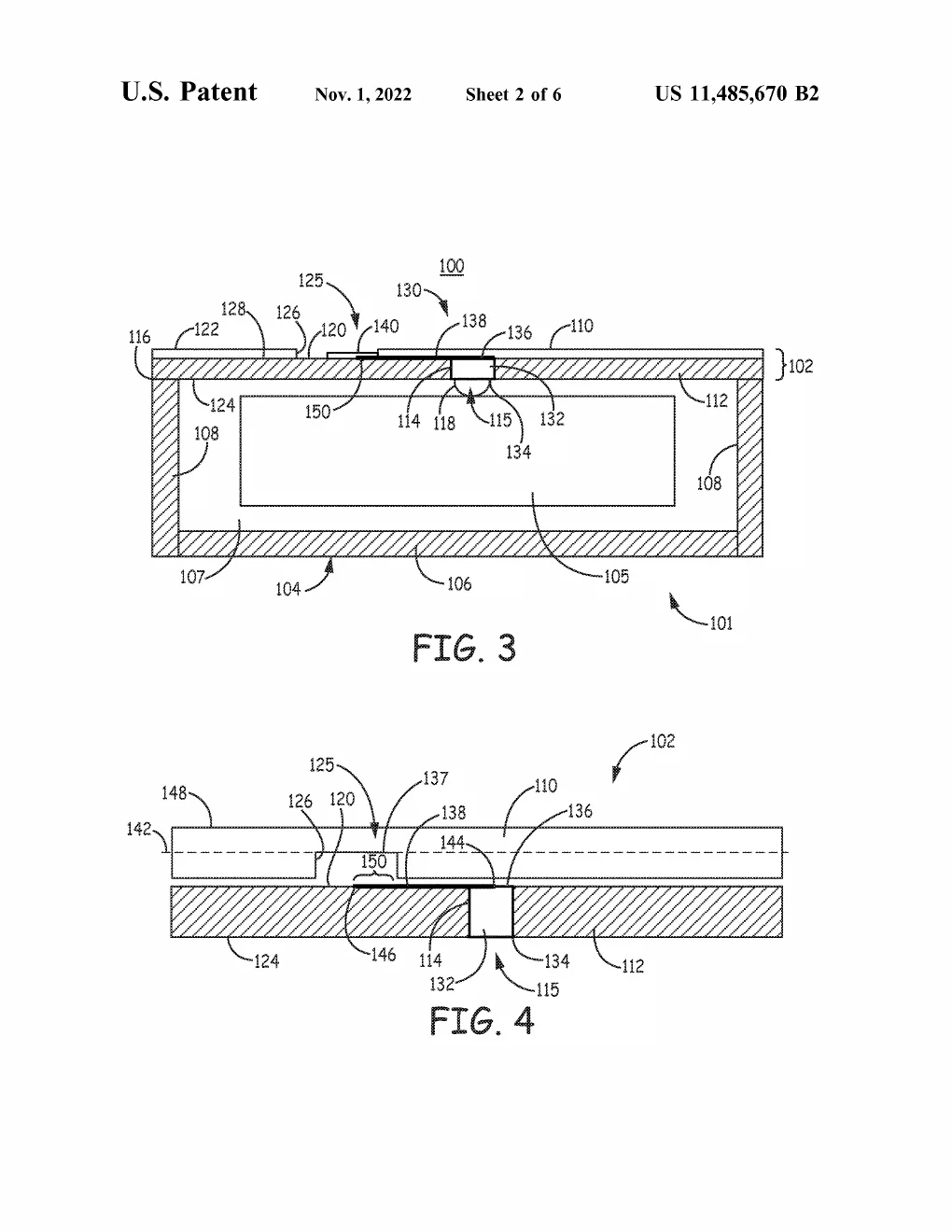
US 11,485,670 · from the drawings Cross-sections of the glass-wafer package: the sealed cavity in full, and a close-up of the buried feedthrough whose conductive trace jogs sideways beneath the surface. -
2023 US 11,548,092 Laser Materials Processing Surface texturing using energy pulses
An implanted electrode wants the most surface area in the least space, but texturing metal in a gas environment can't make the features fine enough. The answer: fire the energy pulses at the metal while it sits under liquid, whose faster heat transfer quenches the melt quickly enough to freeze in texture at micro scale or smaller. The bath does double duty — its oxygen and nitrogen react with the hot metal so texture and surface chemistry arrive in the same pulse, for electrodes, stent struts, and housings.
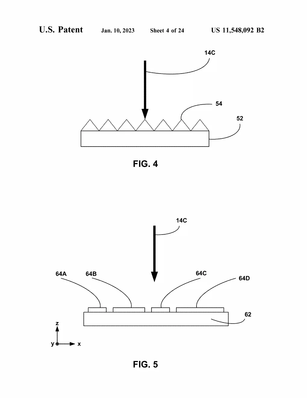
US 11,548,092 · from the drawings An energy pulse strikes the metal surface, leaving a field of micro-scale peaks in its wake. -
US 11,701,503 Flow Control & Surgical Navigation System and method for valve control
For a person with hydrocephalus, an implanted shunt valve quietly decides how much cerebrospinal fluid drains from the brain — the heaviest human stakes anywhere in the corpus. This valve is not a simple spring but a layered machine: tiny MEMS actuators flex a membrane to tune the opening, while a pressure sensor reports back so the implanted controller keeps adjusting until measured flow matches the doctor's target. The settings arrive wirelessly from a handheld programmer outside the body.
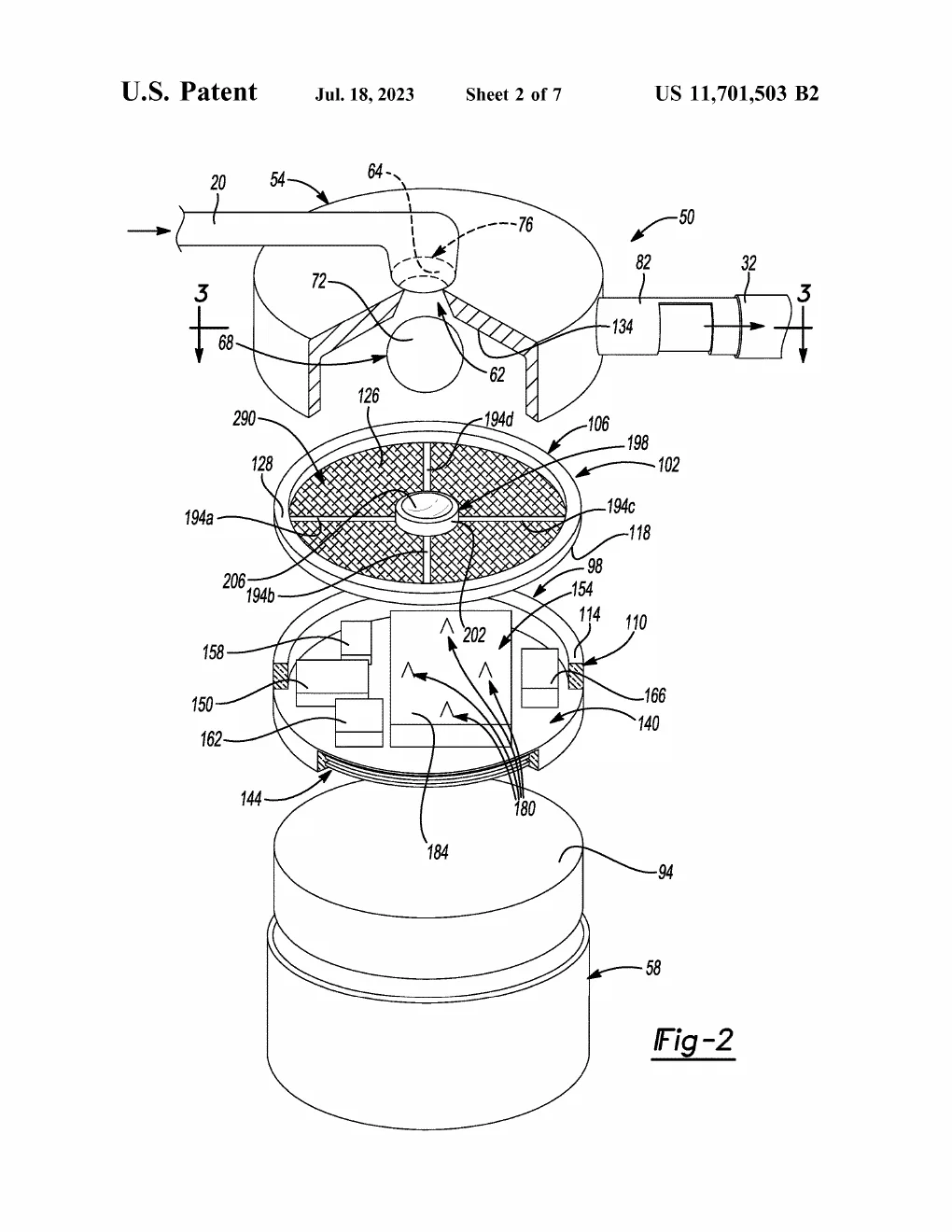
US 11,701,503 · from the drawings The valve assembly pulled apart into its stack: inlet dome with its ball-and-cone seat, the flexible membrane, the plate of MEMS actuators and electronics, and the fluid reservoir base. -
US 11,725,995 Implantable Sensors Pressure sensor assembly for use in implantable medical device (substrate with via along via axis)
Shrink a capacitive pressure sensor far enough and its signal drowns — stray capacitance and manufacturing variation swamp the tiny reading, and protective films only add stress. The fix removes the middleman: the flexing membrane carries one capacitor plate while the second sits on the integrated circuit itself, so the sensing capacitor forms straight along the axis of a via. The membrane can even be part of the enclosure — the sensor's own package becomes the sensing element.
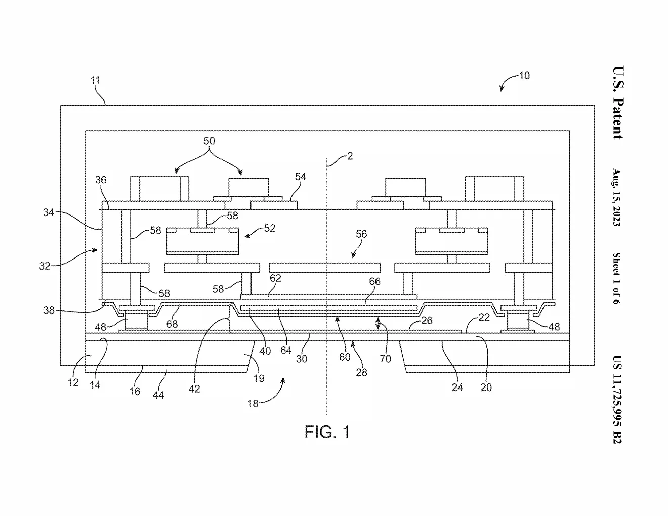
US 11,725,995 · from the drawings A cross-section of the sensor assembly: the flexible membrane spans the substrate via, forming the pressure-sensing gap directly against the circuitry below. -
US 11,744,518 Hermetic Packaging & Feedthroughs Sealed package and method of forming same
Traditional implant housings are built up from ferrules, glass seals, and high-temperature brazing, each one a source of manufacturing complexity and material stress. This grant is the mature form of a different idea: hollow a cavity into the substrate itself, seal a cover layer over it, and laser-bond each electrical contact in a ring around its via — the package is the device body. The laser heats only the surface layer it touches, and the finished bond is stronger than the surrounding material.
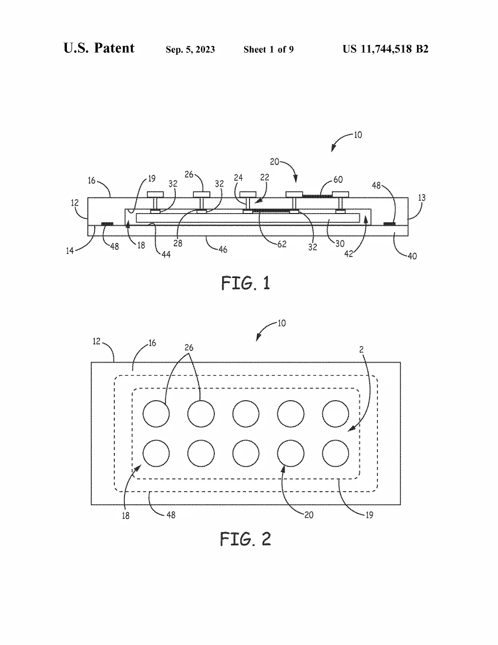
US 11,744,518 · from the drawings A cross-section of the sealed package — electronics enclosed in a cavity between substrate and cover — beside a top view of its grid of feedthrough contacts. -
2024 US 11,865,639 Hermetic Packaging & Feedthroughs Hermetic assembly and device including same
Joining a ceramic-like insulator to a metal frame classically demands either perfectly polished mating surfaces or brazing heat that stresses both parts. The move here is a translator layer: a patterned metal film is laser-bonded onto the insulator first, and the metal ferrule is then conventionally welded to that film — so the fragile insulator never feels the welding heat. And because the bonding works from one side, the frame can be attached after the electronics are already in place, something brazing temperatures would never allow.
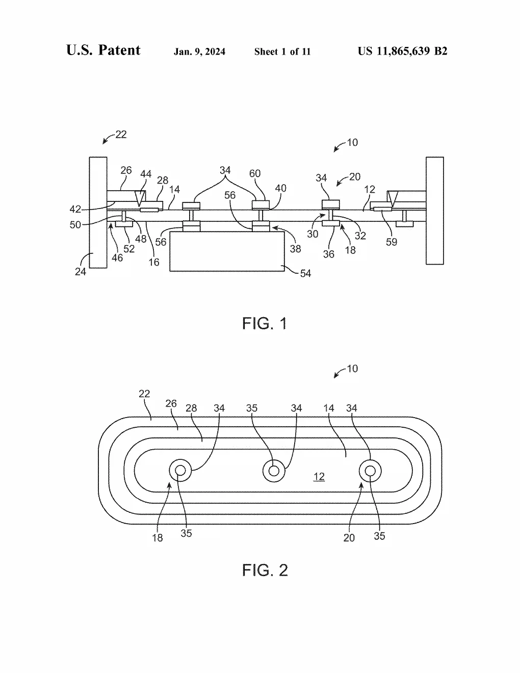
US 11,865,639 · from the drawings A cross-section of the ferrule assembly spanning between housing walls, paired with a top view of the racetrack-shaped frame and its three feedthrough openings. -
US 11,881,325 Power Sources Nuclear radiation particle power converter
A radioisotope is a battery whose lifetime is set by nuclear physics rather than chemistry — the only power source that can promise decades of output sealed inside a body. This grant is the latest and broadest form of the converter: a three-dimensional current collector coated with charge-separating layers, with the radiation-emitting fuel placed so its particles strike inside the sponge rather than a flat panel. It issued in January 2024, just as nuclear microbatteries were making startup headlines, on work with priority stretching back to 2014.
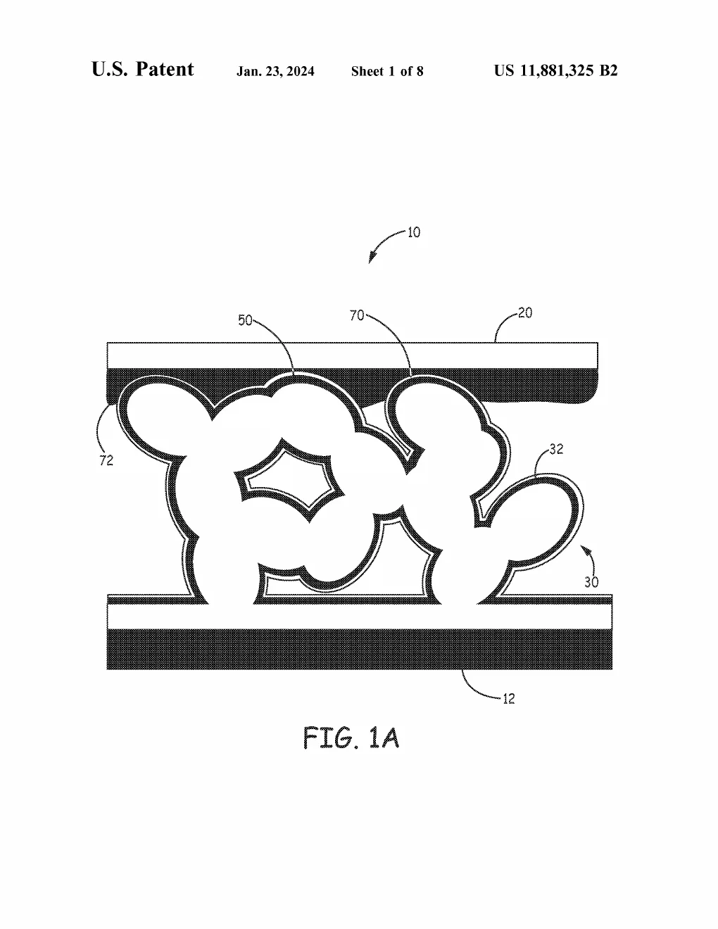
US 11,881,325 · from the drawings A cross-section of the converter: a sponge-like three-dimensional collector, traced with thin coating layers, filling the gap between two flat electrode plates. -
US 11,950,387 Hermetic Packaging & Feedthroughs Methods for forming hermetically-sealed packages including feedthrough assemblies
Every implantable device needs wires to pass through a wall that must stay absolutely sealed against body fluid. This sole-inventor grant covers the methods behind that trick: a laser traces a ring around each tiny via, welding the contact down so the doorway itself is fused shut instead of brazed in a furnace. Granted in 2024, it carried a line seeded by twin provisional applications filed one Christmas Eve in 2014 into its second decade.
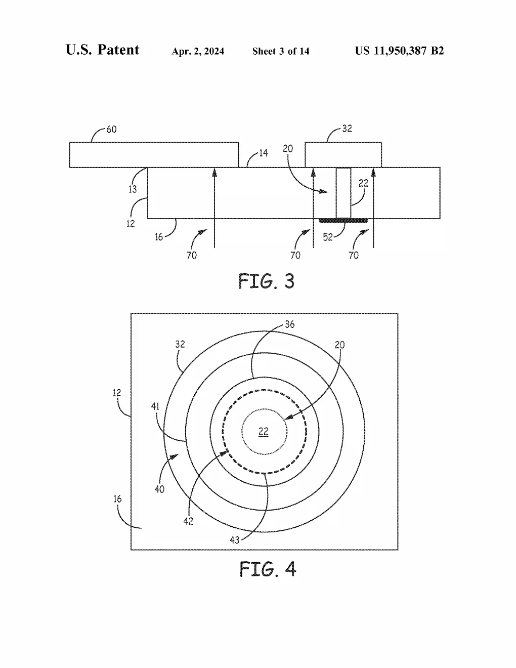
US 11,950,387 · from the drawings Laser energy fires up through the see-through substrate to weld a contact over its tiny via, leaving ring-shaped bond lines encircling the wire's passage. -
US 11,969,821 Laser Materials Processing Surface texturing using energy pulses
An electrode works better the more surface it packs into a tiny footprint, and texturing in a gas environment can't make the features fine enough. The method here fires energy pulses at metal sitting under liquid: the liquid quenches the heat faster, leaving micro-scale-or-smaller texture, while its oxygen and nitrogen react with the hot metal so texture and surface chemistry form in the same pulse. A 2024 continuation of the underwater-texturing line, aimed at electrodes, stent struts, and device housings.
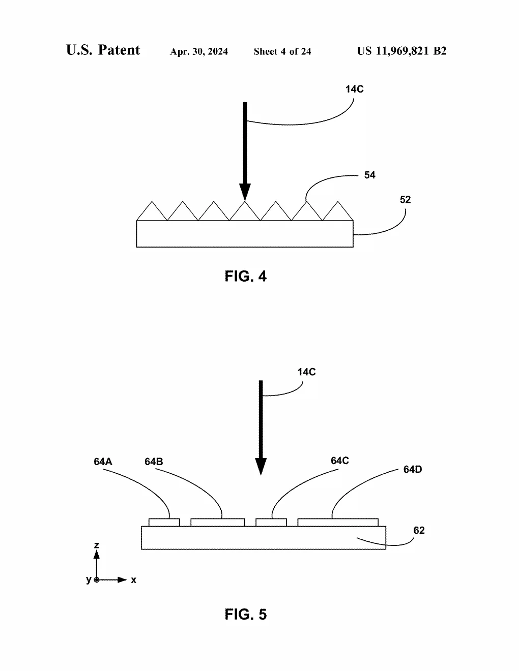
US 11,969,821 · from the drawings A focused pulse of energy strikes the metal, shown in cross-section with the rows of tiny peaks it raises across the surface. -
US 11,999,014 Laser Materials Processing Laser cutting system
Laser-cutting a board with buried conductors has a hidden failure mode: the cut smears conductive residue across the exposed face, leaving invisible paths for leakage. This system cuts with one beam and follows with a second, angled to clean the cut surface — and it watches for the plasma flash when the first beam strikes metal, using that flash to locate the conductor and aim the cleanup beam automatically. Late-career work, granted 2024: even the cutting step gets closed-loop intelligence.
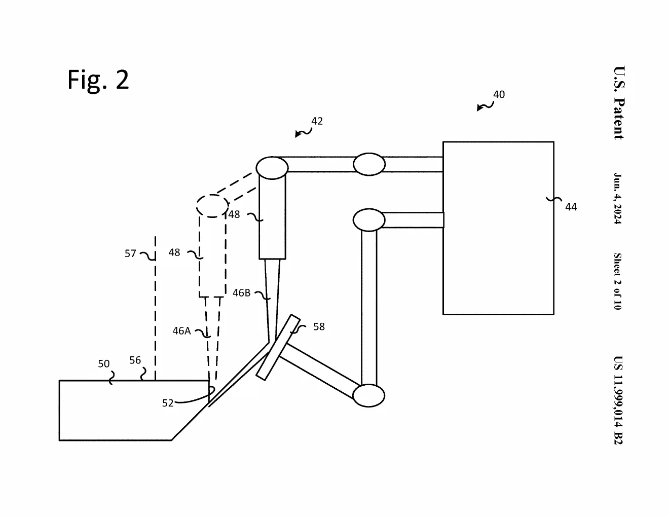
US 11,999,014 · from the drawings Schematic of the two-beam station: the first beam (dashed) slices down through the workpiece, then a mirror redirects the second beam at a controlled angle so it sweeps the freshly cut face. -
US 12,059,542 Flow Control & Surgical Navigation System and method for valve control
In hydrocephalus, excess fluid must drain from the brain through an implanted shunt — and the valve doing that job has to hold exactly the right pressure. This grant continues the closed-loop valve line: a MEMS micro-machine inside the flow-control assembly adjusts the valve according to the selected pressure settings. It belongs to the family the exhibit ranks as carrying the heaviest human stakes in the corpus.
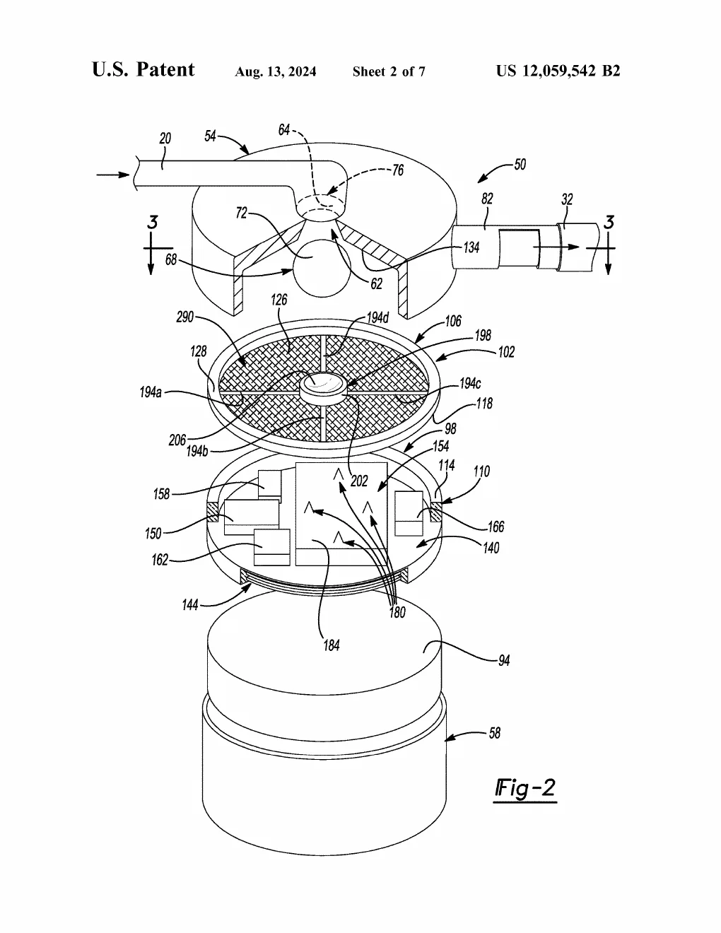
US 12,059,542 · from the drawings Exploded view of the valve assembly: the inlet dome with its ball-and-cone seat on top, the cross-hatched flexible membrane beneath it, the plate of micro-actuators and electronics below, and the fluid reservoir at the base. -
US 12,082,354 Hermetic Packaging & Feedthroughs Electronic package and device including same
A 2024 addition to the hermetic-packaging cluster: an electronic package built around shaped conductor blocks — the scalloped metal pieces at the base of the stack that carry the package's electrical connections. The drawings assemble it like a kit, layer by layer, from the covered components down to the arched blocks beneath the substrate.
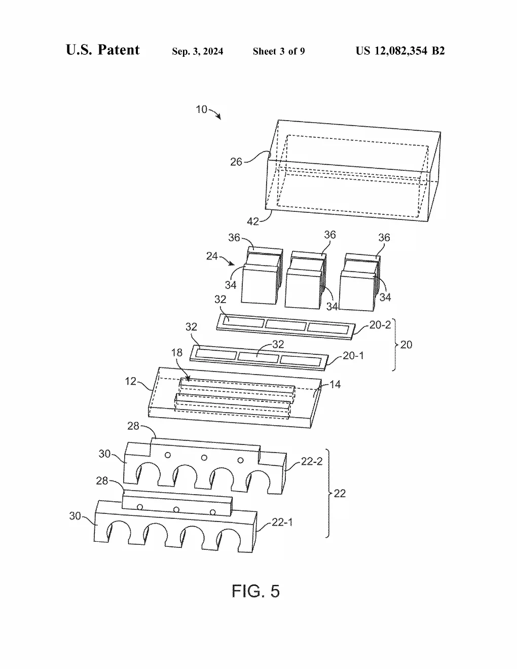
US 12,082,354 · from the drawings Exploded view of the whole package: cover, components, window frames, and substrate stacked above the two rows of arched conductor blocks that carry the connections. -
2025 US 12,233,477 Hermetic Packaging & Feedthroughs Hermetic assembly and device including same
Joining an insulator to a metal frame classically demands perfectly polished mating surfaces or high-temperature brazing that stresses the parts. This 2025 design laser-bonds a patterned metal layer onto the insulator first, then conventionally welds the ferrule's flange to that layer — so the fragile material never feels the welding heat, and because the bonding is one-sided, the frame can be attached after the electronics are already in place. An adapter pattern in metallurgy: one layer translating between the laser-bond world and the weld world.
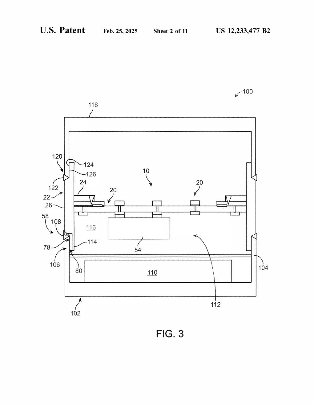
US 12,233,477 · from the drawings Cross-section of the assembly at work: the ferrule-framed insulator plate spans the opening of the device housing, sealing the electronics and power source beneath it. -
US 12,454,117 Laser Materials Processing Kinetically limited nano-scale diffusion bond structures and methods
This is the 2025 form of the diffusion-bond line David shares with glassmaker Corning — one of the few places in the corpus where another company's name sits beside Medtronic's on the patent itself. A laser fires through a transparent material into the buried face where it meets metal, forming a kinetically limited bond only nanometers deep while the bulk of both materials stays cool and undisturbed. The line has drawn 34 citing patent families.
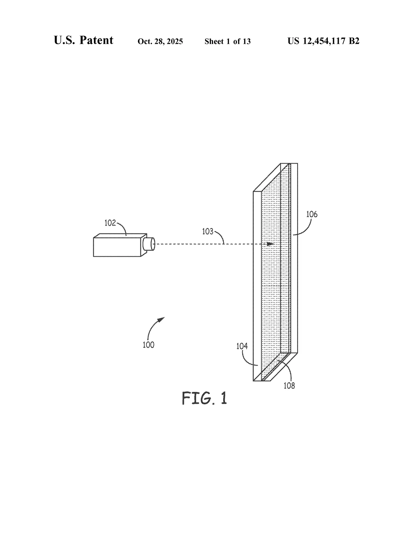
US 12,454,117 · from the drawings The whole setup in one glance: a laser aims its beam at a face-to-face stack of a transparent sheet and a metal plate, landing at the hidden seam between them. -
2026 US 12,610,487 Hermetic Packaging & Feedthroughs Sealed package including electronic device and power source
An implant's insides are full of joints — solder, adhesive, weld — and every one must stay stable for the life of the device. Here the electronics sit on a see-through substrate that is laser-sealed to the housing holding the power source, and the electrical connection between them is never bonded at all: the assembly's own geometry presses the contacts together and keeps them there. It is the newest grant in the corpus, issued April 2026, and 13 patent families already cite it.
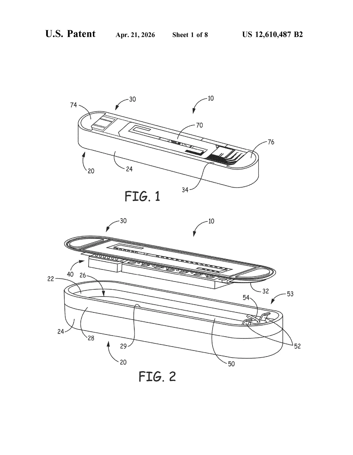
US 12,610,487 · from the drawings The pill-shaped device shown whole, then pulled apart: the electronics carrier lifting away from the housing that holds the power source, with the small spring contact waiting in the far corner where the two simply press together.